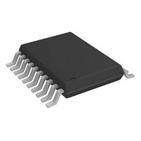
ADG3123BRUZ Analog Devices Inc, ADG3123BRUZ Datasheet - Page 9

ADG3123BRUZ
Manufacturer Part Number
ADG3123BRUZ
Description
IC XLATOR 8CH LOG-HV 20-TSSOP
Manufacturer
Analog Devices Inc
Datasheet
1.ADG3123BRUZ.pdf
(12 pages)
Specifications of ADG3123BRUZ
Logic Function
Translator
Number Of Bits
8
Input Type
CMOS
Output Type
Voltage
Number Of Channels
8
Number Of Outputs/channel
1
Differential - Input:output
No/No
Propagation Delay (max)
125ns
Voltage - Supply
2.3 V ~ 5.5 V
Operating Temperature
-40°C ~ 85°C
Package / Case
20-TSSOP
Supply Voltage
2.3 V ~ 5.5 V
No. Of Inputs
8
Propagation Delay
76ns
Logic Type
Level Translator
Supply Voltage Range
2.3V To 5.5V
Logic Case Style
TSSOP
No. Of Pins
20
Operating Temperature Range
-40°C To +85°C
Lead Free Status / RoHS Status
Lead free / RoHS Compliant
Data Rate
-
Lead Free Status / RoHS Status
Lead free / RoHS Compliant, Lead free / RoHS Compliant
Available stocks
Company
Part Number
Manufacturer
Quantity
Price
Company:
Part Number:
ADG3123BRUZ
Manufacturer:
Analog Devices Inc
Quantity:
1 970
Part Number:
ADG3123BRUZ
Manufacturer:
ADI/亚德诺
Quantity:
20 000
TERMINOLOGY
V
Logic input high voltage at Pin A1 to Pin A8.
V
Logic input low voltage at Pin A1 to Pin A8.
I
Leakage current at Pin A1 to Pin A8.
C
Capacitance measured at Pin A1 to Pin A8.
V
Logic output high voltage at Pin Y1 to Pin Y8.
V
Logic output low voltage at Pin Y1 to Pin Y8.
Ro
Output impedance.
t
Propagation delay through the part measured between the input
signal applied to any one channel and its corresponding output
for a low-to-high transition (see Figure 2).
t
Propagation delay through the part measured between the input
signal applied to any one channel and its corresponding output
for a high-to-low transition (see Figure 2).
t
Rise time of the output signal at Pin Y1 to Pin Y8 (see Figure 2).
PLH
PHL
R
IL
I
IH
IL
OH
OL
Rev. A | Page 9 of 12
t
Fall time of the output signal at the Pin Y1 to Pin Y8
(see Figure 2).
F
Frequency of the signal applied to the A1 to A8 input pins.
V
Input voltage used to generate the high logic levels for Y1 to Y6
outputs.
V
Positive power supply voltage. Also used to generate the high
logic levels for Y7 to Y8 outputs.
V
Negative power supply voltage. It is used to generate the low
logic level for Y1 to Y8 outputs.
GND
Ground (0 V) reference.
I
Supply current at the V
I
Supply current at the V
I
Supply current at the V
F
DDA
DDB
SS
O
DDA
DDB
SS
DDA
DDB
SS
pin.
pin.
pin.
ADG3123


