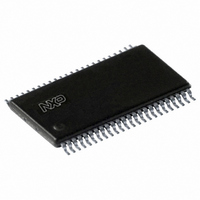
74ALVC16334ADGG;11 NXP Semiconductors, 74ALVC16334ADGG;11 Datasheet - Page 2

74ALVC16334ADGG;11
Manufacturer Part Number
74ALVC16334ADGG;11
Description
IC UNIV BUS DVR 16BIT 48TSSOP
Manufacturer
NXP Semiconductors
Series
74ALVCr
Datasheet
1.74ALVC16334ADGG11.pdf
(12 pages)
Specifications of 74ALVC16334ADGG;11
Logic Type
Universal Bus Driver
Number Of Circuits
16-Bit
Current - Output High, Low
24mA, 24mA
Voltage - Supply
1.2 V ~ 3.6 V
Operating Temperature
-40°C ~ 85°C
Mounting Type
Surface Mount
Package / Case
48-TSSOP
Lead Free Status / RoHS Status
Lead free / RoHS Compliant
Other names
74ALVC16334ADG
74ALVC16334ADG
935267384112
74ALVC16334ADG
935267384112
1. C
Philips Semiconductors
FEATURES
DESCRIPTION
The 74ALVC16334A is a 16–bit universal bus driver. Data flow is
controlled by active low output enable (OE), active low latch enable
(LE) and clock inputs (CP).
When LE is LOW, the A to Y data flow is transparent. When LE is
HIGH and CP is held at LOW or HIGH, the data is latched; on the
LOW to HIGH transient of CP the A-data is stored in the
latch/flip-flop.
When OE is LOW the outputs are active. When OE is HIGH, the
outputs go to the high impedance OFF-state. Operation of the OE
input does not affect the state of the latch/flip-flop.
To ensure the high-impedance state during power up or power
down, OE should be tied to V
minimum value of the resistor is determined by the current-sinking
capability of the driver.
QUICK REFERENCE DATA
GND = 0 V; T
NOTE:
2000 Mar 14
Wide supply voltage range of 1.2 V to 3.6 V
Complies with JEDEC standard no. 8-1A.
CMOS low power consumption
Direct interface with TTL levels
Current drive
MULTIBYTE
Low inductance multiple V
and ground bounce
Output drive capability 50
Input diodes to accommodate strong drivers
16-bit registered driver with inverted register enable
(3-State)
t
F
C
C
C
C
PHL
P
f
SYMBOL
o
max
I
I/O
PD
PD
D
= output frequency in MHz; V
= C
/t
PLH
is used to determine the dynamic power dissipation (P
PD
amb
TM
V
CC
= 25 C; t
24 mA at 3.0 V
flow-through standard pin-out architecture
Propagation delay
An to Yn;
LE to Yn;
CP to Yn
Maximum clock frequency
Input capacitance
Input/Output capacitance
Power dissipation capacitance per buffer
Power dissipation capacitance per buffer
2
f
i
+
r
= t
CC
(C
CC
f
transmission lines @ 85 C
L
and GND pins for minimum noise
through a pullup resistor; the
2.5 ns
PARAMETER
V
CC
CC
= supply voltage in V;
2
f
o
) where: f
i
= input frequency in MHz; C
D
(C
in W):
L
V
V
V = GND to V
V
CC
CC
I
= GND to V
V
CC
= 3.3 V, C
= 3.3 V, C
2
2
PIN CONFIGURATION
f
o
) = sum of outputs.
CC
CC
L
L
= 50 pF
= 50 pF
1
1
L
CONDITIONS
= output load capacitance in pF;
GND
GND
GND
GND
V
V
Y
Y
Y
Y
Y
Y
OE
Y
NC
CC
CC
transparent mode
Y
Y
Y
Y
Y
Y
Y
Y
Y
10
12
13
14
15
16
11
1
2
3
4
5
6
7
8
9
Output disabled
Output disabled
Output enabled
Output enabled
Clocked mode
10
12
13
14
15
16
17
18
19
20
21
22
23
24
11
1
2
3
4
5
6
7
8
9
74ALVC16334A
48
47
46
45
44
43
42
41
40
39
38
37
36
35
34
33
32
31
30
29
28
27
26
25
SH00198
TYPICAL
CP
A
A
GND
A
A
V
A
A
GND
A
A
A
A
GND
A
A
V
A
A
GND
A
A
LE
Product specification
350
1
2
3
4
CC
5
6
7
8
9
10
11
12
CC
13
14
15
16
2.3
2.6
2.5
4.0
8.0
13
22
15
3
853–2196 23314
UNIT
MHz
pF
pF
pF
pF
ns


