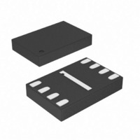
M95320-RMB6TG STMicroelectronics, M95320-RMB6TG Datasheet - Page 21

M95320-RMB6TG
Manufacturer Part Number
M95320-RMB6TG
Description
IC EEPROM 32KBIT 5MHZ 8MLP
Manufacturer
STMicroelectronics
Datasheet
1.M95320-WMN6TP.pdf
(44 pages)
Specifications of M95320-RMB6TG
Format - Memory
EEPROMs - Serial
Memory Type
EEPROM
Memory Size
32K (4K x 8)
Speed
5MHz
Interface
SPI, 3-Wire Serial
Voltage - Supply
1.8 V ~ 5.5 V
Operating Temperature
-40°C ~ 85°C
Package / Case
8-MLP, 8-UFDFPN
Organization
4 K x 8
Interface Type
SPI
Maximum Clock Frequency
5 MHz
Access Time
80 ns
Supply Voltage (max)
5.5 V
Supply Voltage (min)
1.8 V
Maximum Operating Current
3 mA
Maximum Operating Temperature
+ 85 C
Mounting Style
SMD/SMT
Minimum Operating Temperature
- 40 C
Operating Supply Voltage
2.5 V, 3.3 V, 5 V
Memory Configuration
4096 X 8
Clock Frequency
5MHz
Supply Voltage Range
1.8V To 5.5V
Memory Case Style
DFN
No. Of Pins
8
Rohs Compliant
Yes
Lead Free Status / RoHS Status
Lead free / RoHS Compliant
Other names
497-8713-2
M95320-RMB6TG
M95320-RMB6TG
Available stocks
Company
Part Number
Manufacturer
Quantity
Price
Part Number:
M95320-RMB6TG
Manufacturer:
ST
Quantity:
20 000
M95320, M95320-W, M95320-R
6.5
Figure 10. Write Status Register (WRSR) sequence
Read from Memory Array (READ)
As shown in
low. The bits of the instruction byte and address bytes are then shifted in, on Serial Data
Input (D). The address is loaded into an internal address register, and the byte of data at
that address is shifted out, on Serial Data Output (Q).
If Chip Select (S) continues to be driven low, the internal address register is automatically
incremented, and the byte of data at the new address is shifted out.
When the highest address is reached, the address counter rolls over to zero, allowing the
Read cycle to be continued indefinitely. The whole memory can, therefore, be read with a
single READ instruction.
The Read cycle is terminated by driving Chip Select (S) high. The rising edge of the Chip
Select (S) signal can occur at any time during the cycle.
The first byte addressed can be any byte within any page.
The instruction is not accepted, and is not executed, if a Write cycle is currently in progress.
Figure 11. Read from Memory Array (READ) sequence
1. Depending on the memory size, as shown in
S
C
D
Q
S
C
D
Q
0
Figure
1
High Impedance
2
Instruction
3
11, to send this instruction to the device, Chip Select (S) is first driven
4
0
5
1
High Impedance
6
2
Instruction
Doc ID 5711 Rev 12
7
3
MSB
15
8
4
14 13
9 10
5
16-Bit Address
Table
6
7
MSB
6, the most significant address bits are Don’t Care.
3
20 21 22 23 24 25 26 27
7
8
2
6
9 10 11 12 13 14 15
1
5
Register In
0
4
Status
MSB
7
3
6
2
5
1
Data Out 1
4
0
3
28 29 30
AI02282D
2
1
31
0
Instructions
7
Data Out 2
AI01793D
21/44


