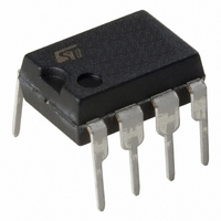
M24C32-WBN6P STMicroelectronics, M24C32-WBN6P Datasheet - Page 30

M24C32-WBN6P
Manufacturer Part Number
M24C32-WBN6P
Description
IC EEPROM 32KBIT 400KHZ 8DIP
Manufacturer
STMicroelectronics
Specifications of M24C32-WBN6P
Format - Memory
EEPROMs - Serial
Memory Type
EEPROM
Memory Size
32K (4K x 8)
Speed
400kHz
Interface
I²C, 2-Wire Serial
Voltage - Supply
2.5 V ~ 5.5 V
Operating Temperature
-40°C ~ 85°C
Package / Case
8-DIP (0.300", 7.62mm)
Organization
4 K x 8
Interface Type
I2C
Maximum Clock Frequency
0.4 MHz
Access Time
900 ns
Supply Voltage (max)
5.5 V
Supply Voltage (min)
2.5 V
Maximum Operating Current
2 mA
Maximum Operating Temperature
+ 85 C
Mounting Style
Through Hole
Minimum Operating Temperature
- 40 C
Operating Supply Voltage
2.5 V, 5.5 V
Memory Configuration
4096 X 8
Clock Frequency
400kHz
Supply Voltage Range
2.5V To 5.5V
Memory Case Style
DIP
No. Of Pins
8
Rohs Compliant
Yes
Lead Free Status / RoHS Status
Lead free / RoHS Compliant
Other names
497-8571
M24C32-WBN6P
M24C32-WBN6P
Available stocks
Company
Part Number
Manufacturer
Quantity
Price
DC and AC parameters
30/42
Table 16.
1. Test conditions (in addition to those in
2. Characterized only, not tested in production.
3. With C
4. There is no min. or max. values for the input signal rise and fall times. It is however recommended by the
5. The new M24C32 device (identified by the process letter K) offers t
6. To avoid spurious Start and Stop conditions, a minimum delay is placed between SCL=1 and the falling or
7. t
8. The current M24C32 device offers t
t
t
CLQV
Symbol
QL1QL2
t
t
XH1XH2
XL1XL2
t
t
t
t
t
t
t
t
t
CHDH
I²C specification that the input signal rise and fall times be more than 20 ns and less than 300 ns when
f
(min), while the current device offers t
safe margin compared to the I
rising edge of SDA.
0.7V
letter K) offers t
recommended by the I
CHCL
CLCH
DXCX
CLDX
CLQX
CHDL
DHDL
DLCL
C
CLQV
t
t
f
NS
W
C
< 400 kHz.
(6)(7)
CC
(2)
is the time (from the falling edge of SCL) required by the SDA bus line to reach either 0.3V
L
, assuming that R
= 10 pF.
t
t
t
t
t
SU:STO
SU:DAT
HD:DAT
SU:STA
HD:STA
400 kHz AC characteristics
t
t
f
t
HIGH
Alt.
t
LOW
t
t
SCL
BUF
WR
t
DH
t
t
AA
R
F
F
NS
=80 ns (min). Both products offer a safe margin compared to the 50 ns minimum value
Clock frequency
Clock pulse width high
Clock pulse width low
SDA (out) fall time
Input signal rise time
Input signal fall time
Data in set up time
Data in hold time
Data out hold time
Clock low to next data valid (access time)
Start condition setup time
Start condition hold time
Stop condition set up time
Time between Stop condition and next Start
condition
Write time
Pulse width ignored (input filter on SCL and
SDA) - single glitch
2
C specification.
bus
× C
2
C specification which recommends t
bus
Doc ID 4578 Rev 18
time constant is within the values specified in
NS
CLQX
=100 ns (min), the new M24C32 device (identified by the process
Table
Parameter
= 200 ns (min) and t
7,
Table
M24C32-DF, M24C32-W, M24C32-R, M24C32-F
(1)
8,
Table 9
CLQV
and
CLQX
CLQV
Table
= 200 ns (min). Both series offer a
= 100 ns (min) and t
= 0 ns (min).
10).
100
100
1300
1300
20
Min.
600
100
600
600
600
(4)
(4)
Figure
0
(3)
(5)
(5)
4.
CLQV
Max.
80
400
120
900
(4)
(4)
5
(8)
CC
= 100 ns
or
Unit
kHz
ms
ns
ns
ns
ns
ns
ns
ns
ns
ns
ns
ns
ns
ns
ns


