M27W401-80K6 STMicroelectronics, M27W401-80K6 Datasheet - Page 8
M27W401-80K6
Manufacturer Part Number
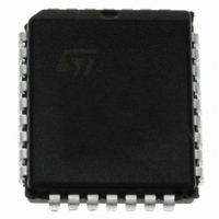
M27W401-80K6
Description
IC OTP 4MBIT 80NS 32PLCC
Manufacturer
STMicroelectronics
Datasheet
1.M27W401-80K6.pdf
(23 pages)
Specifications of M27W401-80K6
Format - Memory
EPROMs
Memory Type
OTP EPROM
Memory Size
4M (512K x 8)
Speed
80ns
Interface
Parallel
Voltage - Supply
2.7 V ~ 3.6 V
Operating Temperature
-40°C ~ 85°C
Package / Case
32-PLCC
Density
4Mb
Organization
512Kx8
Interface Type
Parallel
Bus Type
Parallel
In System Programmable
External
Access Time (max)
80ns
Package Type
PLCC
Reprogramming Technique
OTP
Operating Supply Voltage (typ)
3.3V
Operating Supply Voltage (min)
2.7V
Operating Supply Voltage (max)
3.6V
Supply Current
50mA
Pin Count
32
Mounting
Surface Mount
Operating Temp Range
-40C to 85C
Operating Temperature Classification
Industrial
Lead Free Status / RoHS Status
Lead free / RoHS Compliant
Other names
497-1693-5
Available stocks
Company
Part Number
Manufacturer
Quantity
Price
Company:

Part Number:
M27W401-80K6
Manufacturer:
DIODES
Quantity:
67 000
Company:
Part Number:
M27W401-80K6
Manufacturer:
STMicroelectronics
Quantity:
10 000


Device description
2
Note:
2.1
2.2
2.3
8/23
Device description
Table 2
read mode. All inputs are TTL levels except for V
Table 2.
X = V
Read mode
The M27W401 has two control functions, both of which must be logically active in order to
obtain data at the outputs. Chip Enable (E) is the power control and should be used for
device selection. Output Enable (G) is the output control and should be used to gate data to
the output pins, independent of device selection. Assuming that the addresses are stable,
the address access time (t
available at the output after a delay of t
been low and the addresses have been stable for at least t
Standby mode
The M27W401 has a standby mode which reduces the supply current from 15mA to 15µA
with low voltage operation V
The M27W401 is placed in the standby mode by applying a CMOS high signal to the E
input. When in the standby mode, the outputs are in a high impedance state, independent of
the G input.
Two-line output control
Because EPROMs are usually used in larger memory arrays, this product features a 2 line
control function which accommodates the use of multiple memory connection. The two line
control function allows:
For the most efficient use of these two control lines, E should be decoded and used as the
primary device selecting function, while G should be made a common connection to all
Read
Output Disable
Program
Verify
Program Inhibit
Standby
Electronic Signature
the lowest possible memory power dissipation,
complete assurance that output bus contention will not occur.
IH
lists the operating modes of the M27W40. A single power supply is required in the
Mode
or V
IL
Operating modes
, V
ID
= 12V ± 0.5V.
V
IL
AVQV
V
V
V
V
V
V
Pulse
E
IH
IH
IH
IL
IL
IL
CC
) is equal to the delay from E to output (t
3.6V, see Read Mode DC Characteristics table for details.
GLQV
V
V
V
V
V
V
G
X
IH
IH
IH
IL
IL
IL
from the falling edge of G, assuming that E has
PP
and 12V on A9 for Electronic Signature.
V
A9
X
X
X
X
X
X
ID
AVQV
-t
GLQV
V
V
V
CC
CC
CC
V
V
V
V
V
.
or V
or V
or V
CC
PP
PP
PP
PP
ELQV
SS
SS
SS
). Data is
Data Out
Data Out
M27W401
Data In
Q7-Q0
Codes
Hi-Z
Hi-Z
Hi-Z
Related parts for M27W401-80K6
Image
Part Number
Description
Manufacturer
Datasheet
Request
R

Part Number:
Description:
Manufacturer:
STMicroelectronics
Datasheet:

Part Number:
Description:
4 Mbit (512Kb x 8) Low Voltage UV EPROM and OTP EPROM
Manufacturer:
STMICROELECTRONICS [STMicroelectronics]
Datasheet:
Part Number:
Description:
4 Mbit 512Kb x 8 Low Voltage UV EPROM and OTP EPROM
Manufacturer:
STMICROELECTRONICS [STMicroelectronics]
Datasheet:

Part Number:
Description:
IC OTP 4KBIT 80NS 32DIP
Manufacturer:
STMicroelectronics
Datasheet:
Part Number:
Description:
IC OTP 4KBIT 80NS 32CDIP
Manufacturer:
STMicroelectronics
Datasheet:

Part Number:
Description:
IC OTP 4KBIT 80NS 32TSOP
Manufacturer:
STMicroelectronics
Datasheet:
Part Number:
Description:
4 Mbit 512kb X 8 Low Voltage Uv Eprom And Otp Eprom
Manufacturer:
STMicroelectronics
Datasheet:
Part Number:
Description:
4 Mbit 512Kb x 8 Low Voltage UV EPROM and OTP EPROM
Manufacturer:
STMicroelectronics
Datasheet:
Part Number:
Description:
4 Mbit 512Kb x 8 Low Voltage UV EPROM and OTP EPROM
Manufacturer:
STMicroelectronics
Datasheet:
Part Number:
Description:
STMicroelectronics [RIPPLE-CARRY BINARY COUNTER/DIVIDERS]
Manufacturer:
STMicroelectronics
Datasheet:
Part Number:
Description:
STMicroelectronics [LIQUID-CRYSTAL DISPLAY DRIVERS]
Manufacturer:
STMicroelectronics
Datasheet:

Part Number:
Description:
BOARD EVAL FOR MEMS SENSORS
Manufacturer:
STMicroelectronics
Datasheet: