M27C64A-10F1 STMicroelectronics, M27C64A-10F1 Datasheet - Page 2
M27C64A-10F1
Manufacturer Part Number
M27C64A-10F1
Description
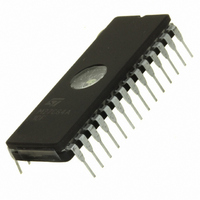
IC EPROM 64KBIT 100NS 28CDIP
Manufacturer
STMicroelectronics
Specifications of M27C64A-10F1
Format - Memory
EPROMs
Memory Type
UV EPROM
Memory Size
64K (8K x 8)
Speed
100ns
Interface
Parallel
Voltage - Supply
4.5 V ~ 5.5 V
Operating Temperature
0°C ~ 70°C
Package / Case
28-CDIP (0.600", 15.24mm) Window
Memory Configuration
8K X 8
Access Time
100ns
Supply Voltage Range
4.5V To 5V
Memory Case Style
DIP
No. Of Pins
28
Rohs Compliant
Yes
Lead Free Status / RoHS Status
Lead free / RoHS Compliant
Other names
497-1684-5
Available stocks
Company
Part Number
Manufacturer
Quantity
Price
Company:

Part Number:
M27C64A-10F1
Manufacturer:
MICROCHIP
Quantity:
1 200
Company:
Part Number:
M27C64A-10F1
Manufacturer:
ST
Quantity:
6 100
Company:
Part Number:
M27C64A-10F1
Manufacturer:
ST
Quantity:
6 100
Part Number:
M27C64A-10F1
Manufacturer:
ST
Quantity:
20 000


M27C64A
Figure 2A. DIP Connections
Table 1. Signal Names
2/14
A0-A12
Q0-Q7
E
G
P
V
V
V
NC
DU
PP
CC
SS
V PP
V SS
A12
Q0
Q1
Q2
A7
A6
A5
A4
A3
A2
A1
A0
1
2
3
4
5
6
7
8
9
10
11
12
13
14
M27C64A
Address Inputs
Data Outputs
Chip Enable
Output Enable
Program
Program Supply
Supply Voltage
Ground
Not Connected Internally
Don’t Use
AI00835
28
27
26
25
24
23
22
21
20
19
18
17
16
15
V CC
P
NC
A8
A9
A11
G
A10
E
Q7
Q6
Q5
Q4
Q3
Figure 2B. Pin Connections
DEVICE OPERATION
The modes of operation of the M27C64A are listed
in the Operating Modes table. A single power sup-
ply is required in the read mode. All inputs are TTL
levels except for V
Signature.
Read Mode
The M27C64A has two control functions, both of
which must be logically active in order to obtain
data at the outputs. Chip Enable (E) is the power
control and should be used for device selection.
Output Enable (G) is the output control and should
be used to gate data to the output pins, indepen-
dent of device selection. Assuming that the ad-
dresses are stable, the address access time
(t
(t
of t
E has been low and the addresses have been sta-
ble for at least t
AVQV
ELQV
GLQV
). Data is available at the output after a delay
) is equal to the delay from E to output
NC
Q0
A6
A5
A4
A3
A2
A1
A0
from the falling edge of G, assuming that
9
AVQV
PP
M27C64A
-t
and 12V on A9 for Electronic
GLQV
17
1
32
.
25
AI00836
A8
A9
A11
NC
G
A10
E
Q7
Q6
Related parts for M27C64A-10F1
Image
Part Number
Description
Manufacturer
Datasheet
Request
R

Part Number:
Description:
IC EPROM 64KBIT 150NS 28CDIP
Manufacturer:
STMicroelectronics
Datasheet:
Part Number:
Description:
IC EPROM 64KBIT 200NS 28CDIP
Manufacturer:
STMicroelectronics
Datasheet:
Part Number:
Description:
IC EPROM 64KBIT 200NS 28CDIP
Manufacturer:
STMicroelectronics
Datasheet:

Part Number:
Description:
64K (8K x 8) UV EPROM and OTP ROM
Manufacturer:
STMICROELECTRONICS [STMicroelectronics]
Datasheet:
Part Number:
Description:
64 Kbit (8Kb x8) UV EPROM and OTP EPROM
Manufacturer:
STMICROELECTRONICS [STMicroelectronics]
Datasheet:

Part Number:
Description:
64 Kbit 8Kb x 8 UV EPROM and OTP EPROM
Manufacturer:
STMicroelectronics
Datasheet:
Part Number:
Description:
STMicroelectronics [RIPPLE-CARRY BINARY COUNTER/DIVIDERS]
Manufacturer:
STMicroelectronics
Datasheet:
Part Number:
Description:
STMicroelectronics [LIQUID-CRYSTAL DISPLAY DRIVERS]
Manufacturer:
STMicroelectronics
Datasheet:

Part Number:
Description:
BOARD EVAL FOR MEMS SENSORS
Manufacturer:
STMicroelectronics
Datasheet:
Part Number:
Description:
NPN TRANSISTOR POWER MODULE
Manufacturer:
STMicroelectronics
Datasheet:
Part Number:
Description:
TURBOSWITCH ULTRA-FAST HIGH VOLTAGE DIODE
Manufacturer:
STMicroelectronics
Datasheet:
Part Number:
Description:
Manufacturer:
STMicroelectronics
Datasheet: