M27C64A-10F1 STMicroelectronics, M27C64A-10F1 Datasheet - Page 8
M27C64A-10F1
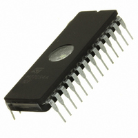
Manufacturer Part Number
M27C64A-10F1
Description
IC EPROM 64KBIT 100NS 28CDIP
Manufacturer
STMicroelectronics
Specifications of M27C64A-10F1
Format - Memory
EPROMs
Memory Type
UV EPROM
Memory Size
64K (8K x 8)
Speed
100ns
Interface
Parallel
Voltage - Supply
4.5 V ~ 5.5 V
Operating Temperature
0°C ~ 70°C
Package / Case
28-CDIP (0.600", 15.24mm) Window
Memory Configuration
8K X 8
Access Time
100ns
Supply Voltage Range
4.5V To 5V
Memory Case Style
DIP
No. Of Pins
28
Rohs Compliant
Yes
Lead Free Status / RoHS Status
Lead free / RoHS Compliant
Other names
497-1684-5
Available stocks
Company
Part Number
Manufacturer
Quantity
Price
Company:

Part Number:
M27C64A-10F1
Manufacturer:
MICROCHIP
Quantity:
1 200
Company:
Part Number:
M27C64A-10F1
Manufacturer:
ST
Quantity:
6 100
Company:
Part Number:
M27C64A-10F1
Manufacturer:
ST
Quantity:
6 100
Part Number:
M27C64A-10F1
Manufacturer:
ST
Quantity:
20 000


M27C64A
Table 10. Programming Mode DC Characteristics
(T
Note: 1. V
Table 11. Programming Mode AC Characteristics
(T
Note: 1. V
Programming
When delivered (and after each erasure for UV
EPROM), all bits of the M27C64A are in the "1"
state. Data is introduced by selectively program-
ming "0"s into the desired bit locations. Although
only "0"s will be programmed, both "1"s and "0"s
can be present in the data word. The only way to
8/14
A
A
t
Symbol
GHQZ
t
t
t
t
t
t
t
VPHPL
VCHPL
t
t
t
= 25 °C; V
= 25 °C; V
PHQX
QXGL
GLQV
GHAX
Symbol
QVPL
AVPL
PLPH
ELPL
2. Sampled only, not 100% tested.
V
V
I
V
V
I
V
I
CC
PP
OH
LI
OL
IH
ID
IL
(2)
CC
CC
must be applied simultaneously with or before V
must be applied simultaneously with or before V
CC
CC
t
t
t
t
t
t
t
t
Alt
t
t
VPS
VCS
CES
OES
DFP
t
PW
DS
DH
OE
AH
AS
Input Leakage Current
Supply Current
Program Current
Input Low Voltage
Input High Voltage
Output Low Voltage
Output High Voltage TTL
A9 Voltage
= 6V ± 0.25V; V
= 6V ± 0.25V; V
Address Valid to Program Low
Input Valid to Program Low
V
V
Chip Enable Low to Program Low
Program Pulse Width (Initial)
Program Pulse Width (Over Program)
Program High to Input Transition
Input Transition to Output Enable Low
Output Enable Low to Output Valid
Output Enable High to Output Hi-Z
Output Enable High to Address
Transition
PP
CC
High to Program Low
High to Program Low
Parameter
PP
PP
Parameter
= 12.5V ± 0.25V)
= 12.5V ± 0.25V)
PP
PP
and removed simultaneously or after V
and removed simultaneously or after V
Test Condition
V
(1)
I
(1)
OH
I
IL
OL
change a "0" to a "1" is by die exposition to ultravi-
olet light (UV EPROM). The M27C64A is in the
programming mode when V
is at V
grammed is applied to 8 bits in parallel to the data
output pins. The levels required for the address
and data inputs are TTL. V
± 0.25V.
E = V
= –400µA
= 2.1mA
V
IN
Test Condition
IL
IL
V
and P is pulsed to V
IH
–0.3
11.5
Min
2.4
2
PP
PP
.
0.95
2.85
.
Min
CC
2
2
2
2
2
2
2
0
0
V
PP
IL
CC
. The data to be pro-
is specified to be 6V
Max
12.5
±10
0.8
0.4
30
30
input is at 12.5V, E
+ 0.5
78.75
Max
1.05
100
130
Unit
mA
mA
µA
V
V
V
V
V
Unit
ms
ms
µs
µs
µs
µs
µs
µs
µs
ns
ns
ns
Related parts for M27C64A-10F1
Image
Part Number
Description
Manufacturer
Datasheet
Request
R

Part Number:
Description:
IC EPROM 64KBIT 150NS 28CDIP
Manufacturer:
STMicroelectronics
Datasheet:
Part Number:
Description:
IC EPROM 64KBIT 200NS 28CDIP
Manufacturer:
STMicroelectronics
Datasheet:
Part Number:
Description:
IC EPROM 64KBIT 200NS 28CDIP
Manufacturer:
STMicroelectronics
Datasheet:

Part Number:
Description:
64K (8K x 8) UV EPROM and OTP ROM
Manufacturer:
STMICROELECTRONICS [STMicroelectronics]
Datasheet:
Part Number:
Description:
64 Kbit (8Kb x8) UV EPROM and OTP EPROM
Manufacturer:
STMICROELECTRONICS [STMicroelectronics]
Datasheet:

Part Number:
Description:
64 Kbit 8Kb x 8 UV EPROM and OTP EPROM
Manufacturer:
STMicroelectronics
Datasheet:
Part Number:
Description:
STMicroelectronics [RIPPLE-CARRY BINARY COUNTER/DIVIDERS]
Manufacturer:
STMicroelectronics
Datasheet:
Part Number:
Description:
STMicroelectronics [LIQUID-CRYSTAL DISPLAY DRIVERS]
Manufacturer:
STMicroelectronics
Datasheet:

Part Number:
Description:
BOARD EVAL FOR MEMS SENSORS
Manufacturer:
STMicroelectronics
Datasheet:
Part Number:
Description:
NPN TRANSISTOR POWER MODULE
Manufacturer:
STMicroelectronics
Datasheet:
Part Number:
Description:
TURBOSWITCH ULTRA-FAST HIGH VOLTAGE DIODE
Manufacturer:
STMicroelectronics
Datasheet:
Part Number:
Description:
Manufacturer:
STMicroelectronics
Datasheet: