M27C64A-20F1 STMicroelectronics, M27C64A-20F1 Datasheet - Page 8
M27C64A-20F1
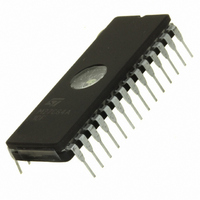
Manufacturer Part Number
M27C64A-20F1
Description
IC EPROM 64KBIT 200NS 28CDIP
Manufacturer
STMicroelectronics
Specifications of M27C64A-20F1
Format - Memory
EPROMs
Memory Type
UV EPROM
Memory Size
64K (8K x 8)
Speed
200ns
Interface
Parallel
Voltage - Supply
4.5 V ~ 5.5 V
Operating Temperature
0°C ~ 70°C
Package / Case
28-CDIP (0.600", 15.24mm) Window
Capacitance, Input
6 pF
Capacitance, Output
12 pF
Current, Input, Leakage
±10 μA (Read)
Current, Operating
30 mA (Read)
Current, Output, Leakage
±10 μA (Read)
Current, Supply
30 mA (Max.)
Density
64K
Organization
8K×8
Package Type
FDIP28W
Temperature, Operating
0 to +70 °C
Temperature, Operating, Maximum
85 °C
Temperature, Operating, Minimum
-40 °C
Time, Access
200 ns
Time, Fall
≤20 ns
Time, Rise
≤20 ns
Voltage, Input, High
6 V (Read)
Voltage, Input, High Level
2 V (Min.)
Voltage, Input, Low
0.8 V (Read)
Voltage, Input, Low Level
-0.3 V (Max.)
Voltage, Output, High
4.3 V (Read)
Voltage, Output, Low
0.4 V (Read)
Voltage, Programmable
11.5 V (Min.)
Voltage, Supply
5 V
Lead Free Status / RoHS Status
Lead free / RoHS Compliant
Other names
497-1686-5
Available stocks
Company
Part Number
Manufacturer
Quantity
Price
Company:

Part Number:
M27C64A-20F1
Manufacturer:
OMRON
Quantity:
2 000
Company:
Part Number:
M27C64A-20F1
Manufacturer:
ST
Quantity:
8 000
Company:
Part Number:
M27C64A-20F1
Manufacturer:
ST
Quantity:
8 000
Part Number:
M27C64A-20F1
Manufacturer:
MBM
Quantity:
20 000


Device operation
2
2.1
2.2
2.3
2.4
8/22
Device operation
The modes of operation of the M27C64A are listed in the Operating Modes table. A single
power supply is required in the read mode. All inputs are TTL levels except for V
on A9 for Electronic Signature.
Read mode
The M27C64A has two control functions, both of which must be logically active in order to
obtain data at the outputs. Chip Enable (E) is the power control and should be used for
device selection. Output Enable (G) is the output control and should be used to gate data to
the output pins, independent of device selection. Assuming that the addresses are stable,
the address access time (t
available at the output after a delay of t
been low and the addresses have been stable for at least t
Standby mode
The M27C64A has a standby mode which reduces the active current from 30mA to 100µA.
The M27C64A is placed in the standby mode by applying a CMOS high signal to the E input.
When in the standby mode, the outputs are in a high impedance state, independent of the G
input.
Two Line output control
Because EPROMs are usually used in larger memory arrays, this product features a 2 line
control function which accommodates the use of multiple memory connection. The two line
control function allows:
For the most efficient use of these two control lines, E should be decoded and used as the
primary device selecting function, while G should be made a common connection to all
devices in the array and connected to the READ line from the system control bus. This
ensures that all deselected memory devices are in their low power standby mode and that
the output pins are only active when data is required from a particular memory device.
System considerations
The power switching characteristics of Advanced CMOS EPROMs require careful
decoupling of the devices. The supply current, I
the system designer: the standby current level, the active current level, and transient current
peaks that are produced by the falling and rising edges of E. The magnitude of the transient
current peaks is dependent on the capacitive and inductive loading of the device at the
output. The associated transient voltage peaks can be suppressed by complying with the
two line output control and by properly selected decoupling capacitors. It is recommended
that a 0.1µF ceramic capacitor be used on every device between V
The lowest possible memory power dissipation
Complete assurance that output bus contention will not occur
AVQV
) is equal to the delay from E to output (t
GLQV
from the falling edge of G, assuming that E has
CC
, has three segments that are of interest to
AVQV
-t
GLQV
CC
.
and V
ELQV
SS
). Data is
. This should
PP
M27C64A
and 12V
Related parts for M27C64A-20F1
Image
Part Number
Description
Manufacturer
Datasheet
Request
R

Part Number:
Description:
IC EPROM 64KBIT 150NS 28CDIP
Manufacturer:
STMicroelectronics
Datasheet:
Part Number:
Description:
IC EPROM 64KBIT 100NS 28CDIP
Manufacturer:
STMicroelectronics
Datasheet:
Part Number:
Description:
IC EPROM 64KBIT 200NS 28CDIP
Manufacturer:
STMicroelectronics
Datasheet:

Part Number:
Description:
64K (8K x 8) UV EPROM and OTP ROM
Manufacturer:
STMICROELECTRONICS [STMicroelectronics]
Datasheet:
Part Number:
Description:
64 Kbit (8Kb x8) UV EPROM and OTP EPROM
Manufacturer:
STMICROELECTRONICS [STMicroelectronics]
Datasheet:

Part Number:
Description:
64 Kbit 8Kb x 8 UV EPROM and OTP EPROM
Manufacturer:
STMicroelectronics
Datasheet:
Part Number:
Description:
STMicroelectronics [RIPPLE-CARRY BINARY COUNTER/DIVIDERS]
Manufacturer:
STMicroelectronics
Datasheet:
Part Number:
Description:
STMicroelectronics [LIQUID-CRYSTAL DISPLAY DRIVERS]
Manufacturer:
STMicroelectronics
Datasheet:

Part Number:
Description:
BOARD EVAL FOR MEMS SENSORS
Manufacturer:
STMicroelectronics
Datasheet:
Part Number:
Description:
NPN TRANSISTOR POWER MODULE
Manufacturer:
STMicroelectronics
Datasheet:
Part Number:
Description:
TURBOSWITCH ULTRA-FAST HIGH VOLTAGE DIODE
Manufacturer:
STMicroelectronics
Datasheet:
Part Number:
Description:
Manufacturer:
STMicroelectronics
Datasheet: