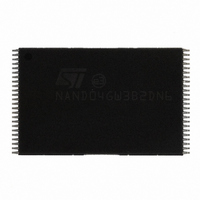
NAND04GW3B2DN6E NUMONYX, NAND04GW3B2DN6E Datasheet - Page 18

NAND04GW3B2DN6E
Manufacturer Part Number
NAND04GW3B2DN6E
Description
IC FLASH 4GBIT 48TSOP
Manufacturer
NUMONYX
Datasheet
1.NAND04GW3B2DN6E.pdf
(72 pages)
Specifications of NAND04GW3B2DN6E
Format - Memory
FLASH
Memory Type
FLASH - Nand
Memory Size
4G (512M x 8)
Interface
Parallel
Voltage - Supply
2.7 V ~ 3.6 V
Operating Temperature
-40°C ~ 85°C
Package / Case
48-TSOP
Lead Free Status / RoHS Status
Lead free / RoHS Compliant
Speed
-
Lead Free Status / RoHS Status
Lead free / RoHS Compliant
Available stocks
Company
Part Number
Manufacturer
Quantity
Price
Company:
Part Number:
NAND04GW3B2DN6E
Manufacturer:
StarMicro
Quantity:
872
Company:
Part Number:
NAND04GW3B2DN6E
Manufacturer:
ST
Quantity:
5 645
Part Number:
NAND04GW3B2DN6E
Manufacturer:
ST
Quantity:
20 000
Bus operations
4
4.1
4.2
4.3
4.4
18/72
Bus operations
There are six standard bus operations that control the memory, as described in this section.
SeeTable 5: Bus operations
Typically, glitches of less than 5 ns on Chip Enable, Write Enable, and Read Enable are
ignored by the memory and do not affect bus operations.
Command input
Command input bus operations give commands to the memory.
Commands are accepted when Chip Enable is Low, Command Latch Enable is High,
Address Latch Enable is Low, and Read Enable is High. They are latched on the rising edge
of the Write Enable signal.
Only I/O0 to I/O7 are used to input commands.
See
Address input
Address input bus operations input the memory addresses. Five bus cycles are required to
input the addresses (refer to
insertion (x16
The addresses are accepted when Chip Enable is Low, Address Latch Enable is High,
Command Latch Enable is Low, and Read Enable is High. They are latched on the rising
edge of the Write Enable signal.
Only I/O0 to I/O7 are used to input addresses.
See
Data input
Data input bus operations input the data to be programmed.
Data is accepted only when Chip Enable is Low, Address Latch Enable is Low, Command
Latch Enable is Low, and Read Enable is High. The data is latched on the rising edge of the
Write Enable signal. The data is input sequentially using the Write Enable signal.
See
Data output
Data output bus operations read the data in the memory array, the status register, the
electronic signature, and the unique identifier.
Data is output when Chip Enable is Low, Write Enable is High, Address Latch Enable is Low,
and Command Latch Enable is Low.
The data is output sequentially using the Read Enable signal.
Figure 24
Figure 25
Figure 26
devices)).
and
and
and
Table 30
Table 30
Table 30
for a summary of these operations.
for details of the timings requirements.
for details of the timings requirements.
and
Table 6: Address insertion (x8 devices)
Table 31
for details of the timings requirements.
NAND04G-B2D, NAND08G-BxC
and
Table 7: Address


