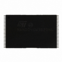
NAND04GW3B2DN6E NUMONYX, NAND04GW3B2DN6E Datasheet - Page 34

NAND04GW3B2DN6E
Manufacturer Part Number
NAND04GW3B2DN6E
Description
IC FLASH 4GBIT 48TSOP
Manufacturer
NUMONYX
Datasheet
1.NAND04GW3B2DN6E.pdf
(72 pages)
Specifications of NAND04GW3B2DN6E
Format - Memory
FLASH
Memory Type
FLASH - Nand
Memory Size
4G (512M x 8)
Interface
Parallel
Voltage - Supply
2.7 V ~ 3.6 V
Operating Temperature
-40°C ~ 85°C
Package / Case
48-TSOP
Lead Free Status / RoHS Status
Lead free / RoHS Compliant
Speed
-
Lead Free Status / RoHS Status
Lead free / RoHS Compliant
Available stocks
Company
Part Number
Manufacturer
Quantity
Price
Company:
Part Number:
NAND04GW3B2DN6E
Manufacturer:
StarMicro
Quantity:
872
Company:
Part Number:
NAND04GW3B2DN6E
Manufacturer:
ST
Quantity:
5 645
Part Number:
NAND04GW3B2DN6E
Manufacturer:
ST
Quantity:
20 000
Device operations
6.8
Figure 19. Multiplane block erase
1. This address scheme refers to x8 devices. Please remember to use the appropriate scheme for x16 devices.
34/72
I/O 0-7
RB
CL
W
AL
R
RB
I/O
Block Erase
Setup code
60h R1
Multiplane block erase
The multiplane block erase operation allows the erasure of two blocks in parallel, one in
each plane.
This operation consists of the following three steps (refer to
erase):
1.
2.
If the multiplane block erase fails, an error is signaled on bit SR0 of the status register. To
know which page of the two planes failed, the Read Status Enhanced command must be
issued twice, once for each plane (see
60h
A
10 bus cycles are required to set up the Block Erase command and load the addresses
of the blocks to be erased. The setup command followed by the address of the block to
be erased must be issued for each block. t
insertion of first and the second block addresses. As for multiplane page program
operations, the address of the first and second page must be within the first plane
(A18 = 0 for x8 devices, A17 = 0 for x16 devices) and second plane (A18 = 1 for x8
devices, A17 = 1 for x16 devices), respectively.
1 bus cycle is then required to issue the Multiplane Block Erase Confirm command and
start the P/E/R controller.
R2
A
A12-A17=0
Block address
A17-A29=0
R3
A18=0
inputs
A
D1h
tIPBSY
Busy
a) Traditional sequence
b) ONFI 1.0 sequence.
Block Erase
Setup code
60h
60h R1
Section
B
Block address
R2
A17-A29=valid
IEBSY
6.12).
A12-A17=0
B
A18=1
inputs
R3
(Program Busy time)
B
busy time is required between the
D0h
tBLBH2
Confirm
NAND04G-B2D, NAND08G-BxC
D0h
code
Figure 19: Multiplane block
Busy
(Erase Busy time)
tBLBH3
Busy
70h
Read Status
register
ai13173c
SR0


