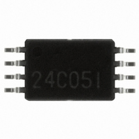
CAT24C05YI-GT3 ON Semiconductor, CAT24C05YI-GT3 Datasheet - Page 3

CAT24C05YI-GT3
Manufacturer Part Number
CAT24C05YI-GT3
Description
IC EEPROM 4KBIT 400KHZ 8TSSOP
Manufacturer
ON Semiconductor
Datasheet
1.CAT24C03YI-GT3.pdf
(14 pages)
Specifications of CAT24C05YI-GT3
Format - Memory
EEPROMs - Serial
Memory Type
EEPROM
Memory Size
4K (512 x 8)
Speed
400kHz
Interface
I²C, 2-Wire Serial
Voltage - Supply
1.8 V ~ 5.5 V
Operating Temperature
-40°C ~ 85°C
Package / Case
8-TSSOP
Organization
512 x 8
Interface Type
I2C
Maximum Clock Frequency
0.4 MHz
Access Time
900 ns
Supply Voltage (max)
5.5 V
Supply Voltage (min)
1.8 V
Maximum Operating Current
1 mA
Maximum Operating Temperature
+ 85 C
Mounting Style
SMD/SMT
Minimum Operating Temperature
- 40 C
Operating Supply Voltage
2.5 V, 3.3 V, 5 V
Lead Free Status / RoHS Status
Lead free / RoHS Compliant
Other names
24C05YI-GT3
CAT24C05YI-GT3TR
CAT24C05YI-GT3TR
Available stocks
Company
Part Number
Manufacturer
Quantity
Price
Company:
Part Number:
CAT24C05YI-GT3
Manufacturer:
ON
Quantity:
120
4. These parameters are tested initially and after a design or process change that affects the parameter according to appropriate AEC−Q100
5. When not driven, the WP pin is pulled down to GND internally. For improved noise immunity, the internal pull−down is relatively strong;
6. Test conditions according to “A.C. Test Conditions” table.
7. Tested initially and after a design or process change that affects this parameter.
8. t
Table 4. PIN IMPEDANCE CHARACTERISTICS
(V
Table 5. A.C. CHARACTERISTICS
(Note 6) (V
t
Table 6. A.C. TEST CONDITIONS
PU
Input Levels
Input Rise and Fall Times
Input Reference Levels
Output Reference Levels
Output Load
CC
and JEDEC test methods.
therefore the external driver must be able to supply the pull−down current when attempting to drive the input HIGH. To conserve power, as
the input level exceeds the trip point of the CMOS input buffer (~ 0.5 x V
t
T
PU
F
Symbol
I
i
(Notes 7, 8)
C
t
t
t
t
t
= 1.8 V to 5.5 V, T
t
t
WP
HD:DAT
SU:STO
HD:STA
SU:STA
SU:DAT
(Note 7)
(Note 7)
SU:WP
HD:WP
t
F
t
Symbol
IN
t
is the delay between the time V
HIGH
t
LOW
BUF
t
t
WR
SCL
DH
t
AA
R
(Note 4)
(Note 5)
CC
= 1.8 V to 5.5 V, T
Clock Frequency
START Condition Hold Time
Low Period of SCL Clock
High Period of SCL Clock
START Condition Setup Time
Data In Hold Time
Data In Setup Time
SDA and SCL Rise Time
SDA and SCL Fall Time
STOP Condition Setup Time
Bus Free Time Between STOP and START
SCL Low to Data Out Valid
Data Out Hold Time
Noise Pulse Filtered at SCL and SDA Inputs
WP Setup Time
WP Hold Time
Write Cycle Time
Power−up to Ready Mode
A
SDA I/O Pin Capacitance
Input Capacitance (Other Pins)
WP Input Current
= −40°C to +85°C, unless otherwise specified.)
A
Parameter
= −40°C to +85°C, unless otherwise specified.)
CC
is stable and the device is ready to accept commands.
0.2 x V
v 50 ns
0.3 x V
0.5 x V
Current Source: I
Parameter
CC
CC
CC
, 0.7 x V
to 0.8 x V
http://onsemi.com
OL
CC
CC
= 3 mA (V
3
V
V
V
IN
IN
IN
CC
< V
< V
< V
CC
Conditions
w 2.5 V); I
V
V
V
IH
IH
IH
), the strong pull−down reverts to a weak current source.
IN
IN
IN
, V
, V
, V
= 0 V
= 0 V
> V
CC
CC
CC
IH
= 5.5 V
= 3.3 V
= 1.8 V
OL
Min
250
100
= 1 mA (V
4.7
4.7
4.7
2.5
4
4
0
4
0
Standard
1000
Max
100
300
100
CC
3.5
5
1
< 2.5 V); C
Min
100
100
0.6
1.3
0.6
0.6
0.6
1.3
2.5
0
0
L
Max
Fast
200
150
100
= 100 pF
8
6
1
Max
400
300
300
100
0.9
5
1
Units
Units
kHz
pF
pF
mA
ms
ms
ms
ms
ms
ms
ms
ns
ns
ns
ms
ms
ms
ns
ns
ms
ms


