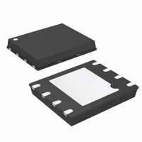
AT45DB081D-MU Atmel, AT45DB081D-MU Datasheet - Page 23

AT45DB081D-MU
Manufacturer Part Number
AT45DB081D-MU
Description
IC FLASH 8MBIT 66MHZ 8VDFN
Manufacturer
Atmel
Datasheet
1.AT45DB081D-MU.pdf
(53 pages)
Specifications of AT45DB081D-MU
Format - Memory
FLASH
Memory Type
DataFLASH
Memory Size
8M (4096 pages x 264 bytes)
Speed
66MHz
Interface
SPI, RapidS
Voltage - Supply
2.7 V ~ 3.6 V
Operating Temperature
-40°C ~ 85°C
Package / Case
8-VFQFN, 8-VFQFPN
Architecture
Sectored
Interface Type
SPI
Supply Voltage (max)
3.6 V
Supply Voltage (min)
2.7 V
Maximum Operating Current
15 mA
Mounting Style
SMD/SMT
Organization
64 KB x 16
Density
8Mb
Access Time (max)
6ns
Boot Type
Not Required
Address Bus
1b
Operating Supply Voltage (typ)
3/3.3V
Operating Temp Range
-40C to 85C
Package Type
MLF EP
Program/erase Volt (typ)
2.7 to 3.6V
Sync/async
Synchronous
Operating Temperature Classification
Industrial
Operating Supply Voltage (min)
2.7V
Operating Supply Voltage (max)
3.6V
Supply Current
15mA
Mounting
Surface Mount
Pin Count
8
Lead Free Status / RoHS Status
Lead free / RoHS Compliant
Available stocks
Company
Part Number
Manufacturer
Quantity
Price
Part Number:
AT45DB081D-MU
Manufacturer:
ATMEL/爱特梅尔
Quantity:
20 000
12.1
13. “Power of 2” Binary Page Size Option
3596M–DFLASH–5/10
Resume from Deep Power-down
The Resume from Deep Power-down command takes the device out of the Deep Power-down
mode and returns it to the normal standby mode. To Resume from Deep Power-down mode, the
CS pin must first be asserted and an opcode of ABH command must be clocked in via input pin
(SI). After the last bit of the command has been clocked in, the CS pin must be de-asserted to
terminate the Deep Power-down mode. After the CS pin is de-asserted, the device will return to
the normal standby mode within the maximum t
the t
down, the device will return to the normal standby mode.
Table 12-2.
Figure 12-2. Resume from Deep Power-Down
“Power of 2” binary page size Configuration Register is a user-programmable nonvolatile regis-
ter that allows the page size of the main memory to be configured for binary page size (256-
bytes) or Atmel
one-time programmable configuration register and once the device is configured for
“power of 2” page size, it cannot be reconfigured again. The devices are initially shipped
with the page size set to 264-bytes. The user has the option of ordering binary page size (256-
bytes) devices from the factory. For details, please refer to
page
For the binary “power of 2” page size to become effective, the following steps must be followed:
If the above steps are not followed in setting the the page size prior to page programming, user
may expect incorrect data during a read operation.
The address format will be changed after the device is configured for “power of 2” page size.
See
(Except Status Register Read, Manufacturer and Device ID Read)” on page
Command
Resume from Deep Power-down
1. Program the one-time programmable configuration resister using opcode sequence
2. Power cycle the device (i.e. power down and power up again).
3. User can now program the page for the binary page size.
RDPD
Section 21.7 ”Command Sequence for Read/Write Operations for Page Size 256-Bytes
47.
3DH, 2AH, 80H and A6H (please see
time before the device can receive any commands. After resuming form Deep Power-
Resume from Deep Power-down
®
DataFlash
®
standard page size (264-bytes). The “power of 2” page size is a
CS
SI
Each transition
represents 8 bits
Section
Opcode
RDPD
13.1).
time. The CS pin must remain high during
Atmel AT45DB081D
Section 26. ”Ordering Information” on
Opcode
ABH
38.
23


