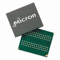
MT48V4M32LFF5-8:G Micron Technology Inc, MT48V4M32LFF5-8:G Datasheet - Page 26

MT48V4M32LFF5-8:G
Manufacturer Part Number
MT48V4M32LFF5-8:G
Description
IC SDRAM 128MBIT 125MHZ 90VFBGA
Manufacturer
Micron Technology Inc
Datasheet
1.MT48LC8M16LFB4-75MG_TR.pdf
(80 pages)
Specifications of MT48V4M32LFF5-8:G
Format - Memory
RAM
Memory Type
Mobile SDRAM
Memory Size
128M (4Mx32)
Speed
125MHz
Interface
Parallel
Voltage - Supply
2.3 V ~ 2.7 V
Operating Temperature
0°C ~ 70°C
Package / Case
90-VFBGA
Lead Free Status / RoHS Status
Contains lead / RoHS non-compliant
Available stocks
Company
Part Number
Manufacturer
Quantity
Price
Company:
Part Number:
MT48V4M32LFF5-8:G
Manufacturer:
MICRON
Quantity:
4 000
Company:
Part Number:
MT48V4M32LFF5-8:G
Manufacturer:
Micron Technology Inc
Quantity:
10 000
Company:
Part Number:
MT48V4M32LFF5-8:G TR
Manufacturer:
Micron Technology Inc
Quantity:
10 000
Operation
BANK/ROW ACTIVATION
Figure 10:
PDF: 09005aef807f4885/Source: 09005aef8071a76b
128Mbx16x32Mobile_2.fm - Rev. M 1/09 EN
Activating a Specific Row in a Specific Bank
Upon exiting the self refresh mode, AUTO REFRESH commands must be issued every
15.625µs or less because both SELF REFRESH and AUTO REFRESH utilize the row
refresh counter.
Self refresh is not supported on automotive temperature (AT) devices.
Before any READ or WRITE commands can be issued to a bank within the SDRAM, a row
in that bank must be “opened.” This is accomplished via the ACTIVE command, which
selects both the bank and the row to be activated (see Figure 10).
After opening a row (issuing an ACTIVE command), a READ or WRITE command may be
issued to that row, subject to the
the clock period and rounded up to the next whole number to determine the earliest
clock edge after the ACTIVE command on which a READ or WRITE command can be
entered. For example, a
results in 2.5 clocks, rounded to 3. This is reflected in Figure 11 on page 27, which covers
any case where 2 <
specification limits from time units to clock cycles.)
A subsequent ACTIVE command to a different row in the same bank can only be issued
after the previous active row has been “closed” (precharged). The minimum time
interval between successive ACTIVE commands to the same bank is defined by
A subsequent ACTIVE command to another bank can be issued while the first bank is
being accessed, which results in a reduction of total row-access overhead. The minimum
time interval between successive ACTIVE commands to different banks is defined by
t
A0–A10, A11
RRD.
BA0, BA1
RAS#
CAS#
WE#
CKE
CLK
CS#
HIGH
t
RCD (MIN)/
t
RCD specification of 20ns with a 125 MHz clock (8ns period)
ADDRESS
ADDRESS
BANK
ROW
26
t
t
CK ≤ 3. (The same procedure is used to convert other
DON’T CARE
RCD specification.
Micron Technology, Inc., reserves the right to change products or specifications without notice.
128Mb: x16, x32 Mobile SDRAM
t
RCD (MIN) should be divided by
©2001 Micron Technology, Inc. All rights reserved.
Register Definition
t
RC.


