TNY256YN Power Integrations, TNY256YN Datasheet - Page 3
TNY256YN
Manufacturer Part Number
TNY256YN
Description
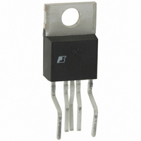
IC OFFLINE SWIT UVLO HV TO220
Manufacturer
Power Integrations
Series
TinySwitch® Plusr
Datasheet
1.TNY256YN.pdf
(20 pages)
Specifications of TNY256YN
Output Isolation
Isolated
Frequency Range
115 ~ 140kHz
Voltage - Output
700V
Power (watts)
11W
Operating Temperature
-40°C ~ 150°C
Package / Case
TO-220-7 (Formed Leads), 5 Leads
Output Voltage
5.8 V
Input / Supply Voltage (max)
265 VAC
Input / Supply Voltage (min)
85 VAC
Duty Cycle (max)
69 %
Switching Frequency
130 KHz
Supply Current
255 uA
Operating Temperature Range
- 40 C to + 150 C
Mounting Style
Through Hole
Lead Free Status / RoHS Status
Lead free / RoHS Compliant
Other names
596-1218-5
TNY256YN
TNY256YN
Available stocks
Company
Part Number
Manufacturer
Quantity
Price
Company:

Part Number:
TNY256YN
Manufacturer:
POWER
Quantity:
15 000
Part Number:
TNY256YN
Manufacturer:
POWER
Quantity:
20 000


TinySwitch Functional Description
TinySwitch combines a high voltage power MOSFET switch
with a power supply controller in one device. Unlike conventional
PWM (Pulse Width Modulator) controllers, TinySwitch uses a
simple ON/OFF control to regulate the output voltage.
The TNY256 controller consists of an Oscillator, Enable (Sense
and Logic) circuit, 5.8 V Regulator, Bypass pin Under-Voltage
circuit, Over Temperature Protection, Current Limit circuit,
Leading Edge Blanking and a 700 V power MOSFET. The
TNY256 incorporates additional circuitry for Line Under-Voltage
Sense, Auto-Restart and Frequency Jitter. Figure 2 shows the
functional block diagram with the most important features.
Oscillator
The typical oscillator frequency is internally set to an average of
130 kHz. Two signals are generated from the oscillator, the
Maximum Duty Cycle signal (DC
indicates the beginning of each cycle.
The TNY256 oscillator incorporates circuitry that introduces a
small amount of frequency jitter, typically 5 kHz peak-to-peak,
to minimize EMI emission. The modulation rate of the frequency
jitter (1 kHz) is set to optimize EMI reduction for both average
and quasi-peak emissions. The frequency jitter should be
measured with the oscilloscope triggered at the falling edge of
the DRAIN waveform. The waveform in Figure4 illustrates the
frequency jitter of the TNY256.
Enable Input Circuit
The enable input circuit at the EN/UV pin consists of a low
impedance source follower output set at 1.5 V. The current
through the source follower is limited to 50 A with 10 A of
hysteresis. When the current drawn out of the this pin exceeds
Figure 4. Frequency Jitter.
400
300
200
100
600
500
0
0
132.5 kHz
127.5 kHz
Time ( s)
V
DRAIN
.5
MAX
) and the Clock signal that
1
50 A, a low logic level (disable) is generated at the output of
the enable circuit. This output is sampled at the beginning of
each cycle on the rising edge of the clock signal. If high, the
power MOSFET is turned on for that cycle (enabled), otherwise
the power MOSFET remains off (disabled). Since the sampling
is done only at the beginning of each cycle, subsequent
changes in the EN/UV pin voltage or current during the
remainder of the cycle are ignored.
Under most operating conditions (except when close to no-
load), the low impedance of the source follower, keeps the
voltage on the EN/UV pin from going much below 1.5 V, in the
disabled state. This improves the response time of the
optocoupler that is usually connected to this pin.
5.8 V Regulator
The 5.8 V regulator charges the bypass capacitor connected to
the BYPASS pin to 5.8 V by drawing a current from the voltage
on the DRAIN, whenever the MOSFET is off. The BYPASS
pin is the internal supply voltage node for the TinySwitch.
When the MOSFET is on, the TinySwitch runs off of the energy
stored in the bypass capacitor.
consumption of the internal circuitry allows the TinySwitch to
operate continuously from the current drawn from the DRAIN
pin. A bypass capacitor value of 0.1 F is sufficient for both
high frequency de-coupling and energy storage.
BYPASS Pin Under-Voltage
The BYPASS pin under-voltage circuitry disables the power
MOSFET when the BYPASS pin voltage drops below 5.1 V.
Once the BYPASS pin voltage drops below 5.1 V, it must rise
back to 5.8 V to enable (turn-on) the power MOSFET.
Over Temperature Protection
The thermal shutdown circuitry senses the die temperature.
The threshold is set at 135
die temperature rises above this threshold (135
MOSFET is disabled and remains disabled until the die
temperature falls by 70
Current Limit
The current limit circuit senses the current in the power
MOSFET. When this current exceeds the internal threshold
(I
that cycle.
The leading edge blanking circuit inhibits the current limit
comparator for a short time (t
turned on. This leading edge blanking time has been set so that
current spikes caused by primary-side capacitance and
secondary-side rectifier reverse recovery time will not cause
premature termination of the switching pulse.
Auto-Restart
In the event of a fault condition such as output overload, output
LIMIT
), the power MOSFET is turned off for the remainder of
o
C, at which point it is re-enabled.
o
C with 70
LEB
) after the power MOSFET is
Extremely low power
o
C hysteresis. When the
TNY256
o
C) the power
7/01
C
3
Related parts for TNY256YN
Image
Part Number
Description
Manufacturer
Datasheet
Request
R

Part Number:
Description:
Energy Efficient, Low Power Off-line Switcher
Manufacturer:
Power Integrations, Inc.
Datasheet:

Part Number:
Description:
SOP-16
Manufacturer:
Power Integrations
Datasheet:
Part Number:
Description:
DIP8
Manufacturer:
Power Integrations
Datasheet:
Part Number:
Description:
TO-263
Manufacturer:
Power Integrations
Datasheet:
Part Number:
Description:
TO-263
Manufacturer:
Power Integrations
Datasheet: