TNY256YN Power Integrations, TNY256YN Datasheet - Page 6
TNY256YN
Manufacturer Part Number
TNY256YN
Description
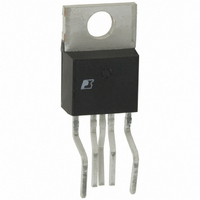
IC OFFLINE SWIT UVLO HV TO220
Manufacturer
Power Integrations
Series
TinySwitch® Plusr
Datasheet
1.TNY256YN.pdf
(20 pages)
Specifications of TNY256YN
Output Isolation
Isolated
Frequency Range
115 ~ 140kHz
Voltage - Output
700V
Power (watts)
11W
Operating Temperature
-40°C ~ 150°C
Package / Case
TO-220-7 (Formed Leads), 5 Leads
Output Voltage
5.8 V
Input / Supply Voltage (max)
265 VAC
Input / Supply Voltage (min)
85 VAC
Duty Cycle (max)
69 %
Switching Frequency
130 KHz
Supply Current
255 uA
Operating Temperature Range
- 40 C to + 150 C
Mounting Style
Through Hole
Lead Free Status / RoHS Status
Lead free / RoHS Compliant
Other names
596-1218-5
TNY256YN
TNY256YN
Available stocks
Company
Part Number
Manufacturer
Quantity
Price
Company:

Part Number:
TNY256YN
Manufacturer:
POWER
Quantity:
15 000
Part Number:
TNY256YN
Manufacturer:
POWER
Quantity:
20 000


200
100
During power-down, when an external resistor is used, the
power MOSFET will switch for 32 ms after the output loses
regulation. The power MOSFET will then remain off without
any glitches since the under-voltage function prohibits restarts
when the line voltage is low.
Figure 10 illustrates a typical power-down timing waveform of
TNY256. Figure 11 illustrates a very slow power-down timing
waveform of TNY256 as in standby applications. The external
resistor (2 M ) is connected to the EN/UV pin in this case to
prevent restarts.
The TNY256 does not require a bias winding to provide power
to the chip, because it draws the power directly from the DRAIN
pin (see Functional Description above). This has two main
benefits. First, for a nominal application, this eliminates the
cost of an extra bias winding and associated components.
Secondly, for charger applications, the current-voltage
characteristic often allows the output voltage to fall to low
values while still delivering power. This type of application
normally requires a forward-bias winding which has many
more associated components, none of which are necessary with
the TNY256.
Current Limit Operation
Each switching cycle is terminated when the DRAIN current
reaches the current limit of the TNY256. For a given primary
inductance and input voltage, the duty cycle is constant.
However, the duty cycle does change inversely with the input
voltage providing “voltage feed-forward” advantages: good
line ripple rejection and relatively constant power delivery
independent of the input voltage.
BYPASS Pin Capacitor
The BYPASS pin uses a small 0.1 F ceramic capacitor for
decoupling the internal power supply of the TNY256.
400
300
200
100
Figure 10. Normal Power-down Timing.
0
0
6
0
TNY256
C
7/01
Time (s)
.5
V
V
DC-BUS
DRAIN
1
Figure 11. Slow Power-down Timing with External (2 M )
Application Example
The TNY256 is ideal for low cost, high efficiency power
supplies in a wide range of applications such as PC standby,
cellular phone chargers, AC adapters, motor control, appliance
control and ISDN network termination. The 130kHz operation
allows the use of a low cost EE16 core transformer while still
providing good efficiency. The frequency jitter in TNY256
makes it possible to use a single inductor (or two small resistors
if lower efficiency is acceptable) in conjunction with two input
capacitors for input EMI filtering up to the 10W level. The
auto-restart function allows the design to be optimized for
maximum efficiency without consideration for short-circuit
current on the secondary. For applications requiring under-
voltage lockout (UVLO), the TNY256 eliminates several
components and saves cost.
As an example, Figure12 shows a 9V, 0.6A, AC adapter
operating from a universal input range (85-265VAC). The AC
input is rectified and filtered by D1-D4, C1 and C2 to create a
high voltage DC bus which is connected to T1. Inductor L1
forms a pi-filter in conjunction with C1 and C2. The resistor R1
damps resonance in inductor L1. The frequency jitter in
TNY256 allows it to meet worldwide conducted EMI standards
using a simple pi-filter in combination with a small value
Y1-capacitor C5 and a shield winding between primary and
secondary windings inside transformer T1. Diode D5, capacitor
C3 and resistor R3 form an RCD clamp circuit that limits the
turn-off voltage spike to a safe value on the TNY256 DRAIN
pin.
The secondary winding is rectified and filtered by D6, C6 and
C7 to provide the 9V output. Additional filtering is provided
by L3 and C8. The output voltage is determined by the resistor
network R7 and R8. Resistor R9 maintains a bias current
200
100
400
300
200
100
0
0
0
Resistor Connected to EN/UV Pin.
Time (s)
2.5
V
V
DC-BUS
DRAIN
5
Related parts for TNY256YN
Image
Part Number
Description
Manufacturer
Datasheet
Request
R

Part Number:
Description:
Energy Efficient, Low Power Off-line Switcher
Manufacturer:
Power Integrations, Inc.
Datasheet:

Part Number:
Description:
SOP-16
Manufacturer:
Power Integrations
Datasheet:
Part Number:
Description:
DIP8
Manufacturer:
Power Integrations
Datasheet:
Part Number:
Description:
TO-263
Manufacturer:
Power Integrations
Datasheet:
Part Number:
Description:
TO-263
Manufacturer:
Power Integrations
Datasheet: