NCP1835MN20R2G ON Semiconductor, NCP1835MN20R2G Datasheet - Page 2
NCP1835MN20R2G
Manufacturer Part Number
NCP1835MN20R2G
Description
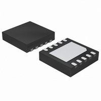
IC BATT CHRGR LI-ION 4.2V 10-DFN
Manufacturer
ON Semiconductor
Type
Battery Chargerr
Datasheet
1.NCP1835MN20R2G.pdf
(16 pages)
Specifications of NCP1835MN20R2G
Function
Charge Management
Battery Type
Lithium-Ion (Li-Ion)
Voltage - Supply
2.8 V ~ 6.5 V
Operating Temperature
-20°C ~ 70°C
Mounting Type
Surface Mount
Package / Case
10-VFDFN Exposed Pad
Output Voltage
4.2 V
Output Current
1000 mA
Operating Supply Voltage
2.8 V to 6.5 V
Maximum Operating Temperature
+ 70 C
Minimum Operating Temperature
- 20 C
Mounting Style
SMD/SMT
Operating Supply Voltage (min)
2.8V
Operating Supply Voltage (max)
6.5V
Operating Temp Range
-20C to 70C
Package Type
DFN
Mounting
Surface Mount
Pin Count
10
Operating Temperature Classification
Commercial
Lead Free Status / RoHS Status
Lead free / RoHS Compliant
Other names
NCP1835MN20R2G
NCP1835MN20R2GOSTR
NCP1835MN20R2GOSTR
Available stocks
Company
Part Number
Manufacturer
Quantity
Price

Part Number:
NCP1835MN20R2G
Manufacturer:
ON/安森美
Quantity:
20 000


PIN FUNCTION DESCRIPTION
Pin
10
1
2
3
4
5
6
7
8
9
Symbol
FAULT
TIMER
VSNS
CFLG
V2P8
GND
ISEL
V
BAT
EN
CC
Input Supply Voltage. Provides power to the charger. This pin should be bypassed with at least a 4.7 mF ceramic
capacitor to ground.
An open−drain output indicating fault status. This pin is pulled LOW under any fault conditions. A FAULT condition
resets the counter.
An open−drain output indicating charging or end−of−charge states. The CFLG pin is pulled LOW when the
charger is charging a battery. It is forced open when the charge current drops to I
will be latched until a recharge cycle or a new charge cycle starts.
Connecting a timing capacitor, C
TIMEOUT = 14*C
TIMEOUT. Trickle Charge has a time limit of 1/8 of the TIMEOUT period.
Ground pin of the IC. For thermal consideration, it is recommended to solder the exposed metal pad on the
backside of the package to ground.
Enable logic input. Connect the EN pin to LOW to disable the charger or leave it floating to enable the charger.
2.8 V reference voltage output. This pin outputs a 2.8 V voltage source when an adapter is present. The
maximum loading for this pin is 2.0 mA.
The full charge current (I
I
I
Battery voltage sense pin. Connect this as close as possible to the battery input connection.
Charge current output. A minimum 4.7 mF capacitor is needed for stability when the battery is not attached.
FCHG
EOC
= (0.1*I
GND
= (0.8*10
V
4.7 mF
in
C
FCHG
V
in
in
5
/ R
TIME
) A. For best accuracy, a resistor with 1% tolerance is recommended.
R
ISEL
Figure 1. Typical Application Circuit
80 k
ISEL
/1.0 nF (minute). The total charge for CC and CV mode is limited to the length of
) A, the pre−charge current I
FCHG
CFLG
FAULT
V
ISEL TIMER
CC
) can be set by connecting a resistor, R
http://onsemi.com
TIME
15 nF
C
between this pin and ground to set end−of−charge timeout timer.
T
VSNS
2
V2P8
GND
BAT
EN
Description
PC
= (0.1*I
0.1 mF
C
2p8
FCHG)
Microprocessor
4.7 mF
C
ISEL
out
A and the end−of−charge threshold current
, from the ISEL pin to ground.
EOC
. This high impedance mode
Related parts for NCP1835MN20R2G
Image
Part Number
Description
Manufacturer
Datasheet
Request
R

Part Number:
Description:
ON Semiconductor [VOLTAGE REGULATOR]
Manufacturer:
ON Semiconductor
Datasheet:
Part Number:
Description:
357-036-542-201 CARDEDGE 36POS DL .156 BLK LOPRO
Manufacturer:
ON Semiconductor
Datasheet:
Part Number:
Description:
357-036-542-201 CARDEDGE 36POS DL .156 BLK LOPRO
Manufacturer:
ON Semiconductor
Datasheet:
Part Number:
Description:
357-036-542-201 CARDEDGE 36POS DL .156 BLK LOPRO
Manufacturer:
ON Semiconductor
Datasheet:
Part Number:
Description:
357-036-542-201 CARDEDGE 36POS DL .156 BLK LOPRO
Manufacturer:
ON Semiconductor
Datasheet:
Part Number:
Description:
357-036-542-201 CARDEDGE 36POS DL .156 BLK LOPRO
Manufacturer:
ON Semiconductor
Datasheet:
Part Number:
Description:
357-036-542-201 CARDEDGE 36POS DL .156 BLK LOPRO
Manufacturer:
ON Semiconductor
Datasheet:
Part Number:
Description:
357-036-542-201 CARDEDGE 36POS DL .156 BLK LOPRO
Manufacturer:
ON Semiconductor
Datasheet:
Part Number:
Description:
357-036-542-201 CARDEDGE 36POS DL .156 BLK LOPRO
Manufacturer:
ON Semiconductor
Datasheet:
Part Number:
Description:
357-036-542-201 CARDEDGE 36POS DL .156 BLK LOPRO
Manufacturer:
ON Semiconductor
Datasheet:
Part Number:
Description:
357-036-542-201 CARDEDGE 36POS DL .156 BLK LOPRO
Manufacturer:
ON Semiconductor
Datasheet:
Part Number:
Description:
Manufacturer:
ON Semiconductor
Datasheet:
Part Number:
Description:
Manufacturer:
ON Semiconductor
Datasheet:
Part Number:
Description:
Manufacturer:
ON Semiconductor
Datasheet: