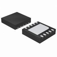
NCP1835MN20R2G ON Semiconductor, NCP1835MN20R2G Datasheet - Page 3

NCP1835MN20R2G
Manufacturer Part Number
NCP1835MN20R2G
Description
IC BATT CHRGR LI-ION 4.2V 10-DFN
Manufacturer
ON Semiconductor
Type
Battery Chargerr
Datasheet
1.NCP1835MN20R2G.pdf
(16 pages)
Specifications of NCP1835MN20R2G
Function
Charge Management
Battery Type
Lithium-Ion (Li-Ion)
Voltage - Supply
2.8 V ~ 6.5 V
Operating Temperature
-20°C ~ 70°C
Mounting Type
Surface Mount
Package / Case
10-VFDFN Exposed Pad
Output Voltage
4.2 V
Output Current
1000 mA
Operating Supply Voltage
2.8 V to 6.5 V
Maximum Operating Temperature
+ 70 C
Minimum Operating Temperature
- 20 C
Mounting Style
SMD/SMT
Operating Supply Voltage (min)
2.8V
Operating Supply Voltage (max)
6.5V
Operating Temp Range
-20C to 70C
Package Type
DFN
Mounting
Surface Mount
Pin Count
10
Operating Temperature Classification
Commercial
Lead Free Status / RoHS Status
Lead free / RoHS Compliant
Other names
NCP1835MN20R2G
NCP1835MN20R2GOSTR
NCP1835MN20R2GOSTR
Available stocks
Company
Part Number
Manufacturer
Quantity
Price
Part Number:
NCP1835MN20R2G
Manufacturer:
ON/安森美
Quantity:
20 000
Stresses exceeding Maximum Ratings may damage the device. Maximum Ratings are stress ratings only. Functional operation above the
Recommended Operating Conditions is not implied. Extended exposure to stresses above the Recommended Operating Conditions may affect
device reliability.
1. This device series contains ESD protection and is tested per the following standards:
2. Latchup Current Maximum Rating: 150 mA per JEDEC standard: JESD78.
3. Measure on 1 inch sq. of 1 oz. copper area. R
4. Moisture Sensitivity Level per IPC/JEDEC standard: J−STD−020A.
MAXIMUM RATINGS
Supply Voltage
Status Flag Output Pins
Voltage Range for Other Pins
Current Out from BAT Pin
Thermal Characteristics
Moisture Sensitivity (Note 4)
Operating Ambient Temperature
Storage Temperature
ESD
Thermal Resistance, Junction−to−Air (Note 3)
Power Dissipation, T
Human Body Model
Machine Model
sq. of 1 oz. copper area on 4 layer PCB that has 1 single signal layer with the additional 3 solid ground or power planes. The maximum package
power dissipation limit must not be exceeded:
with R
P D +
Human Body Model (HBM) per JEDEC standard: JESD22−A114.
Machine Model (MM) per JEDEC standard: JESD22−A115.
qJA
T J(max) * T A
= 68.5°C/W, T
R qJA
FAULT
V2P8
CFLG
V
CC
A
= 25°C (Note 3)
J(max)
VCC
Resistor
Dividers
= 100°C, P
V2P8
Startup,
Control
& Clamp
Rating
VREF
Bias Circuits
Chip
Enable
D
EN
= 1.09 W.
qJA
Figure 2. Detailed Block Diagram
is highly dependent on the PCB heatsink area. For example, R
http://onsemi.com
TIMER
Control
TIMER
LOGIC
3
Temp
CC
CV
V
VREF
FAULT
Symbol
Recharge
Comp
Precharge
Comp
HBM
R
MSL
V
T
MM
V
Timer
Comp
P
T
I
qJA
stg
CC
, V
O
io
A
D
GND
CFLG
IREF
VREF
VREF
VREF
Vbat
Resistor
Dividers
−55 to 125
−20 to 70
Level 1
Value
2000
68.5
1.09
200
7.0
7.0
5.5
1.2
qJA
BAT
ISEL
VSNS
can be 38°C/W on 1 inch
°C/W
Unit
°C
°C
W
V
V
V
A
V
V


