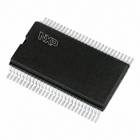
PCF8576T/1,112 NXP Semiconductors, PCF8576T/1,112 Datasheet - Page 14

PCF8576T/1,112
Manufacturer Part Number
PCF8576T/1,112
Description
IC LCD DRV UNVRSL LOW-MUX 56VSOP
Manufacturer
NXP Semiconductors
Datasheet
1.PCF8576T1112.pdf
(44 pages)
Specifications of PCF8576T/1,112
Package / Case
56-VSOP
Mounting Type
Surface Mount
Current - Supply
180µA
Voltage - Supply
2 V ~ 9 V
Operating Temperature
-40°C ~ 85°C
Interface
I²C
Display Type
LCD
Configuration
40 Segment
Lead Free Status / RoHS Status
Lead free / RoHS Compliant
Digits Or Characters
-
Lead Free Status / Rohs Status
Details
Other names
933804620112::PCF8576T/1::PCF8576T/1
Philips Semiconductors
6.5
6.5.1
The internal logic and the LCD drive signals of the
PCF8576 are timed either by the internal oscillator or from
an external clock. When the internal oscillator is used,
pin OSC should be connected to pin V
output from pin CLK provides the clock signal for
cascaded PCF8566s in the system.
Where resistor R
is selected. The relationship between the oscillator
frequency on pin CLK (f
6.5.2
The condition for external clock is made by connecting
pin OSC to pin V
clock input.
The clock frequency (f
frequency and the maximum rate for data reception from
the I
maximum data rate of 100 kHz, f
above 125 kHz.
A clock signal must always be supplied to the device;
removing the clock may freeze the LCD in a DC state.
2001 Oct 02
Universal LCD driver for low multiplex rates
2
f
Fig.9 Oscillator frequency as a function of R
clk
C-bus. To allow I
(kHz)
10
f
10
clk
Oscillator
10
3
2
I
10
E
3.4 10
----------------------- - kHz
NTERNAL CLOCK
XTERNAL CLOCK
2
R
osc
7
osc
DD
; pin CLK then becomes the external
to V
min
clk
2
max
C-bus transmissions at their
SS
clk
) determines the LCD frame
) and R
is present, the internal oscillator
10
3
clk
osc
should be chosen to be
R
is shown in Fig.9.
osc
SS
(k
. In this event, the
MBE531
10
4
osc
.
14
6.6
The timing of the PCF8576 organizes the internal data flow
of the device. This includes the transfer of display data
from the display RAM to the display segment outputs. In
cascaded applications, the synchronization signal SYNC
maintains the correct timing relationship between the
PCF8576s in the system. The timing also generates the
LCD frame frequency which it derives as an integer
multiple of the clock frequency (see Table 2). The frame
frequency is set by the MODE SET commands when
internal clock is used, or by the frequency applied to
pin CLK when external clock is used.
The ratio between the clock frequency and the LCD frame
frequency depends on the mode in which the device is
operating. In the power-saving mode the reduction ratio is
six times smaller; this allows the clock frequency to be
reduced by a factor of six. The reduced clock frequency
results in a significant reduction in power dissipation. The
lower clock frequency has the disadvantage of increasing
the response time when large amounts of display data are
transmitted on the I
When a device is unable to digest a display data byte
before the next one arrives, it holds the SCL line LOW until
the first display data byte is stored. This slows down the
transmission rate of the I
Table 2 LCD frame frequencies
6.7
The display latch holds the display data while the
corresponding multiplex signals are generated. There is a
one-to-one relationship between the data in the display
latch, the LCD segment outputs and one column of the
display RAM.
6.8
The shift register serves to transfer display information
from the display RAM to the display latch while previous
data is displayed.
Normal mode
Power-saving mode
PCF8576 MODE
Timing
Display latch
Shift register
2
C-bus.
FREQUENCY
2
C-bus but no data loss occurs.
FRAME
------------ -
2880
--------- -
480
f
f
clk
clk
Product specification
PCF8576
FREQUENCY
NOMINAL
FRAME
(Hz)
64
64


