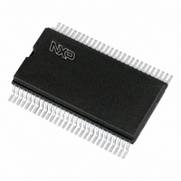
PCF8576T/1,112 NXP Semiconductors, PCF8576T/1,112 Datasheet - Page 15

PCF8576T/1,112
Manufacturer Part Number
PCF8576T/1,112
Description
IC LCD DRV UNVRSL LOW-MUX 56VSOP
Manufacturer
NXP Semiconductors
Datasheet
1.PCF8576T1112.pdf
(44 pages)
Specifications of PCF8576T/1,112
Package / Case
56-VSOP
Mounting Type
Surface Mount
Current - Supply
180µA
Voltage - Supply
2 V ~ 9 V
Operating Temperature
-40°C ~ 85°C
Interface
I²C
Display Type
LCD
Configuration
40 Segment
Lead Free Status / RoHS Status
Lead free / RoHS Compliant
Digits Or Characters
-
Lead Free Status / Rohs Status
Details
Other names
933804620112::PCF8576T/1::PCF8576T/1
Philips Semiconductors
6.9
The LCD drive section includes 40 segment outputs
pins S0 to S39 which should be connected directly to the
LCD. The segment output signals are generated in
accordance with the multiplexed backplane signals and
with data resident in the display latch. When less than
40 segment outputs are required the unused segment
outputs should be left open-circuit.
6.10
The LCD drive section includes four backplane outputs
BP0 to BP3 which should be connected directly to the
LCD. The backplane output signals are generated in
accordance with the selected LCD drive mode. If less than
four backplane outputs are required the unused outputs
can be left open-circuit. In the 1 : 3 multiplex drive mode
BP3 carries the same signal as BP1, therefore these two
adjacent outputs can be connected together to give
enhanced drive capabilities. In the 1 : 2 multiplex drive
mode BP0 and BP2, BP1 and BP3 respectively carry the
same signals and may also be paired to increase the drive
capabilities. In the static drive mode the same signal is
carried by all four backplane outputs and they can be
connected in parallel for very high drive requirements.
6.11
The display RAM is a static 40
LCD data. A logic 1 in the RAM bit-map indicates the on
state of the corresponding LCD segment; similarly, a
logic 0 indicates the off state. There is a one-to-one
2001 Oct 02
Universal LCD driver for low multiplex rates
Fig.10 Display RAM bit-map showing direct relationship between display RAM addresses and segment outputs,
Segment outputs
Backplane outputs
Display RAM
and between bits in a RAM word and backplane outputs.
backplane outputs
display RAM bits
(columns) /
(BP)
4-bit RAM which stores
0
1
2
3
0
1
2
display RAM addresses (rows) / segment outputs (S)
3
4
15
correspondence between the RAM addresses and the
segment outputs, and between the individual bits of a RAM
word and the backplane outputs. The first RAM column
corresponds to the 40 segments operated with respect to
backplane BP0 (see Fig.10). In multiplexed LCD
applications the segment data of the second, third and
fourth column of the display RAM are time-multiplexed
with BP1, BP2 and BP3 respectively.
When display data is transmitted to the PCF8576 the
display bytes received are stored in the display RAM in
accordance with the selected LCD drive mode. To
illustrate the filling order, an example of a 7-segment
numeric display showing all drive modes is given in Fig.11;
the RAM filling organization depicted applies equally to
other LCD types.
With reference to Fig.11, in the static drive mode the eight
transmitted data bits are placed in bit 0 of eight successive
display RAM addresses. In the 1 : 2 multiplex drive mode
the eight transmitted data bits are placed in bits 0 and 1 of
four successive display RAM addresses. In the 1 : 3
multiplex drive mode these bits are placed in
bits 0, 1 and 2 of three successive addresses, with bit 2 of
the third address left unchanged. This last bit may, if
necessary, be controlled by an additional transfer to this
address but care should be taken to avoid overriding
adjacent data because full bytes are always transmitted. In
the 1 : 4 multiplex drive mode the eight transmitted data
bits are placed in bits 0, 1, 2 and 3 of two successive
display RAM addresses.
35
36
37
38
MBE525
39
Product specification
PCF8576


