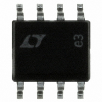
LT1641-1CS8#TR Linear Technology, LT1641-1CS8#TR Datasheet - Page 9

LT1641-1CS8#TR
Manufacturer Part Number
LT1641-1CS8#TR
Description
IC CONTRLR HOTSWAP POSVOLT 8SOIC
Manufacturer
Linear Technology
Type
Hot-Swap Controllerr
Datasheet
1.LT1641-1IS8.pdf
(12 pages)
Specifications of LT1641-1CS8#TR
Applications
General Purpose
Internal Switch(s)
No
Voltage - Supply
9 V ~ 80 V
Operating Temperature
0°C ~ 70°C
Mounting Type
Surface Mount
Package / Case
8-SOIC (0.154", 3.90mm Width)
Lead Free Status / RoHS Status
Contains lead / RoHS non-compliant
Other names
LT1641-1CS8TR
LT16411CS8TR
LT16411CS8TR
Available stocks
Company
Part Number
Manufacturer
Quantity
Price
APPLICATIO S I FOR ATIO
current source. When the TIMER pin falls below 0.5V, the
GATE pin either turns on automatically (LT1641-2) or once
the ON pin is pulsed low to reset the internal fault latch
(LT1641-1).
The waveform in Figure 9 shows how the output latches off
following a short-circuit. The drop across the sense resis-
tor is held at 12mV as the timer ramps up. Since the output
did not rise bringing FB above 0.5V, the circuit latches off.
For Figure 9, C
Undervoltage and Overvoltage Detection
The ON pin can be used to detect an undervoltage condi-
tion at the power supply input. The ON pin is internally
connected to an analog comparator with 80mV of hyster-
esis. If the ON pin falls below its threshold voltage (1.233V),
the GATE pin is pulled low and is held low until ON is high
again.
Figure 10 shows an overvoltage detection circuit. When
the input voltage exceeds the Zener diode’s breakdown
voltage, D2 turns on and starts to pull the TIMER pin high.
After the TIMER pin is pulled higher than 1.233V, the fault
latch is set and the GATE pin is pulled to GND immediately,
turning off transistor Q1. The waveforms are shown in
Figure 11. Operation is restored either by interrupting
power or by pulsing ON low.
Figure 7. Current Limit Sense Voltage vs Feedback Pin Voltage
V
CC
– V
SENSE
47mV
12mV
T
= 100nF.
0V
U
U
0.5V
W
1641-1 F07
V
FB
U
Power Good Detection
The chip includes a comparator for monitoring the output
voltage. The noninverting input (FB pin) is compared
against an internal 1.233V precision reference and exhib-
its 80mV hysteresis. The comparator’s output (PWRGD
pin) is an open collector capable of operating from a pull-
up as high as 100V.
The PWRGD pin can be used to directly enable/disable a
power module with an active high enable input. Figure 12
shows how to use the PWRGD pin to control an active low
enable input power module. Signal inversion is accom-
plished by transistor Q2 and R7.
Supply Transient Protection
The IC is 100% tested and guaranteed to be safe from
damage with supply voltages up to 100V. However, spikes
above 100V may damage the part. During a short-circuit
condition, the large change in currents flowing through
the power supply traces can cause inductive voltage
spikes which could exceed 100V. To minimize the spikes,
the power trace parasitic inductance should be minimized
by using wider traces or heavier trace plating and a 0.1µF
bypass capacitor placed between V
suppressor at the input can also prevent damage from
voltage surges.
12µs
10µs
8µs
6µs
4µs
2µs
PROPAGATION DELAY
Figure 8. Response Time to Overcurrent
50mV
LT1641-1/LT1641-2
100mV
150mV
CC
and GND. A surge
200mV
V
CC
– V
164112fc
1641-1
SENSE
9
F08


