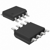
MAX5949BESA+T Maxim Integrated Products, MAX5949BESA+T Datasheet - Page 10

MAX5949BESA+T
Manufacturer Part Number
MAX5949BESA+T
Description
IC CNTRLR HOT SWAP 8-SOIC
Manufacturer
Maxim Integrated Products
Type
Hot-Swap Controllerr
Datasheet
1.MAX5949BESA.pdf
(18 pages)
Specifications of MAX5949BESA+T
Applications
General Purpose
Internal Switch(s)
No
Voltage - Supply
-20 V ~ -80 V
Operating Temperature
-40°C ~ 85°C
Mounting Type
Surface Mount
Package / Case
8-SOIC (0.154", 3.90mm Width)
Lead Free Status / RoHS Status
Lead free / RoHS Compliant
In either case, when the MOSFET is turned off, the out-
put capacitor continues to discharge by the IC supply
current, I
nal, out at the V
through the external MOSFET’s substrate diode. There
is also a parallel current path between the V
DRAIN terminals through multiple internal ESD-protec-
tion diodes. Protection circuits built into the IC allow the
DRAIN terminal voltage to drop below that of the V
terminal so long as the allowed absolute-maximum
DRAIN terminal current (-100mA) is not exceeded. As
I
even be approached.
The MAX5949_ provides current-limiting and circuit-
breaker features that protect against excessive load cur-
rent and short-circuit conditions. The load current is
monitored by sensing the voltage across an external
sense resistor connected between V
If the voltage between V
rent-limit trip voltage (V
the GATE pin and regulates the current through the
external MOSFET so V
drawn by the load drops below V
GATE pin voltage rises again. However, if the load cur-
rent is at the regulation limit of V
of t
MAX5949A/MAX5949B to turn off the external MOSFET.
After an overcurrent fault condition, the circuit breaker
is reset by pulling the UV pin low and then pulling UV
high or by cycling power to the MAX5949A/MAX5949B.
Unless power is cycled to the MAX5949A/MAX5949B,
-48V Hot-Swap Controllers
with External R
Figure 7b. Input Inrush Current
10
DD
PHLCB
is only 2mA maximum, this limiting current will not
______________________________________________________________________________________
DD
, the electronic circuit breaker trips, causing the
. The I
CONTACT
BOUNCE
EE
DD
Current Limit and Electronic
terminal, and back to the capacitor
flows into the IC at the V
SENSE
4ms/div
EE
CL
), the MAX5949_ pulls down
and SENSE reaches the cur-
- V
CL
EE
CL
/ R
EE
< V
Circuit Breaker
/ R
SENSE
SENSE
and SENSE.
CL
SENSE
. If the current
INRUSH
CURRENT
1A/div
GATE - V
10V/div
DRAIN
50V/div
V
50V/div
EE
for a period
DD
EE
limit, the
EE
termi-
and
EE
the device waits until t
on the gate of the external FET.
The MAX5949_ features an overcurrent fault integrator.
When an overcurrent condition exists, an internal digital
counter increments its count. When the counter reaches
500µs (the maximum current-limit duration) for the
MAX5949_, an overcurrent fault is generated. If the
overcurrent fault does not last 500µs, then the counter
begins decrementing at a rate 128 (maximum current-
limit duty cycle) times slower than the counter was
incrementing. Repeated overcurrent conditions will gen-
erate a fault if duty cycle of the overcurrent condition is
greater than 1/128.
The MAX5949_ accomplishes load-current regulation by
pulling current from the GATE pin whenever V
> V
decreases the gate-to-source voltage of the external
MOSFET, thereby reducing the load current. When
V
GATE pin high by a 45µA (I
In the event of a permanent short-circuit condition, the
MAX5949_ limits the current drawn by the load to V
R
breaker trips. Once the circuit breaker trips, the GATE
of the external FET is pulled low by 50mA (I
off power to the load.
The MAX5949_ guards against input voltage steps on the
input supply. A rapid increase in the input supply voltage
(V
C
during an input voltage step, the MAX5949A/MAX5949B
current limit activates, pulling down the gate voltage and
limiting the load current to V
voltage (V
input voltage. As the drain voltage starts to slew down,
the drain-to-gate feedback capacitor C2 pushes back on
the gate, reducing the gate-to-source voltage (V
the current through the external MOSFET. Once the input
supply reaches its final value, the DRAIN slew rate (and
therefore the inrush current) is limited by the capacitor
C2 just as it is limited in the startup condition. To ensure
correct operation, R
current limit larger than the sum of the load current and
the dynamic current into the load capacitance in the
slewing mode.
If the load current plus the capacitive charging current is
below the current limit, the circuit breaker does not trip.
SENSE
SENSE
L
DD
x ∆V
CL
- V
(see the Typical Operating Characteristics). This
IN
- V
EE
for a period of t
/ ∆T. If the load current exceeds V
DRAIN
EE
increasing) causes a current step equal to I =
Immunity to Input Voltage Steps
< V
) then slews at a slower rate than the
CL
Overcurrent Fault Integrator
SENSE
, the MAX5949A/MAX5949B pull the
Driving into a Shorted Load
OFF
Load-Current Regulation
PHLCB
PU
must be chosen to provide a
has elapsed before turning
) current.
CL
, after which the circuit
/ R
SENSE
. The DRAIN
CL
SENSE
PD
/ R
) turning
GS
SENSE
) and
- V
CL
EE
/


