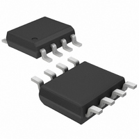
MAX5949BESA+T Maxim Integrated Products, MAX5949BESA+T Datasheet - Page 9

MAX5949BESA+T
Manufacturer Part Number
MAX5949BESA+T
Description
IC CNTRLR HOT SWAP 8-SOIC
Manufacturer
Maxim Integrated Products
Type
Hot-Swap Controllerr
Datasheet
1.MAX5949BESA.pdf
(18 pages)
Specifications of MAX5949BESA+T
Applications
General Purpose
Internal Switch(s)
No
Voltage - Supply
-20 V ~ -80 V
Operating Temperature
-40°C ~ 85°C
Mounting Type
Surface Mount
Package / Case
8-SOIC (0.154", 3.90mm Width)
Lead Free Status / RoHS Status
Lead free / RoHS Compliant
Figure 7a shows a typical hot-swap circuit for -48V sys-
tems. When the circuit board first makes contact with
the backplane, the DRAIN to GATE capacitance (C
of Q1 pulls up the GATE voltage to roughly IV
(C
dynamic clamp between GATE and V
gate-to-source voltage of Q1 low during hot insertion,
preventing Q1 from passing an uncontrolled current to
the load. For most applications, the internal dynamic
clamp between GATE and V
MAX5949B eliminates the need for an external gate-to-
source capacitor C1. Resistor R3 limits the current into
the clamp circuitry during card insertion.
The MAX5949_ can reside either on the backplane or
the removable circuit board (Figure 7a). Power is deliv-
ered to the load by placing an external n-channel
MOSFET pass transistor in the power-supply path.
After the circuit board is inserted into the backplane
and the supply voltage at V
undervoltage and overvoltage tolerance, the MAX5949_
turn on Q1. The MAX5949_ gradually turn on the exter-
nal MOSFET by charging the gate of Q1 with a 45µA
current source.
Figure 7a. Inrush Control Circuitry
gd
+ C
gs
-48V RTN
)I. The MAX5949_ features an internal
*DIODES INC. SMAT70A.
**OPTIONAL.
-48V
*
_______________________________________________________________________________________
(SHORT PIN)
-48V RTN
10nF
Power-Supply Ramping
EE
6.49kΩ
549kΩ
10kΩ
is stable and within the
1%
1%
1%
EE
R4
R5
R6
of the MAX5949A/
Board Insertion
UV
OV
EE
V
EE
to keep the
0.02Ω
5%
EE
R1
x C
SENSE
-48V Hot-Swap Controllers
gd
gd
)
/
MAX5949B
C1**
470nF
25V
V
DD
IRF530
Capacitor C2 provides a feedback signal to accurately
limit the inrush current. The value of C
calculated:
where C
I
Figure 7b shows the inrush current waveform. The cur-
rent through C2 controls the GATE voltage. At the end
of the DRAIN ramp, the GATE voltage is charged to its
final value. The GATE-to-SENSE clamp limits the maxi-
mum V
If the card is removed from a live backplane, the output
capacitor on the card may not be immediately dis-
charged. While the output capacitor is discharging, the
MAX5949_ continues to operate as if the input supply
were still connected because the output capacitor tem-
porarily supplies operating current to the IC. If the cir-
cuit is connected as in Figure 7a, the voltage at the UV
pin falls below the V
the external MOSFET. If R4 in the circuit is connected
directly to the -48V return, the external MOSFET
remains on until the capacitor is discharged sufficiently
to drop the UV pin voltage to V
GATE
PU
Q1
with External R
R2
10Ω
5%
is the MAX5949_ gate pullup current.
1kΩ
5%
R3
GS
L
15nF
100V
to about 18V under any condition.
C2
is the total load capacitance, C3 + C4, and
PWRGD
DRAIN
C
C3
0.1µF
100V
2
UVL
=
I
PU
I
INRUSH
, and the MAX5949_ turns off
C4
100µF
100V
x C
UVL
L
V
V
IN+
IN-
VI-J3D-CY
GATE IN
VICOR
.
Board Removal
SENSE
C5
100µF
10V
2
can be
9


