BD6067GU-E2 Rohm Semiconductor, BD6067GU-E2 Datasheet - Page 25
BD6067GU-E2
Manufacturer Part Number
BD6067GU-E2
Description
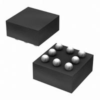
IC LED DRIVR WHITE BCKLGT 8-VCSP
Manufacturer
Rohm Semiconductor
Type
Backlight, White LEDr
Specifications of BD6067GU-E2
Topology
PWM, Step-Up (Boost)
Number Of Outputs
1
Internal Driver
Yes
Type - Primary
Backlight
Type - Secondary
White LED
Frequency
800kHz ~ 1.2MHz
Voltage - Supply
2.7 V ~ 5.5 V
Voltage - Output
30V
Mounting Type
Surface Mount
Package / Case
8-VCSP
Operating Temperature
-30°C ~ 85°C
Current - Output / Channel
30mA
Internal Switch(s)
Yes
Led Driver Application
Mobile Phones
No. Of Outputs
1
Output Current
30mA
Output Voltage
36V
Input Voltage
2.7V To 5.5V
Operating Temperature Range
-30°C To +85°C
Driver
RoHS Compliant
Lead Free Status / RoHS Status
Lead free / RoHS Compliant
Efficiency
-
Lead Free Status / Rohs Status
Details
Other names
BD6067GU-E2TR
Available stocks
Company
Part Number
Manufacturer
Quantity
Price
Company:

Part Number:
BD6067GU-E2
Manufacturer:
RICOH
Quantity:
3 000
Part Number:
BD6067GU-E2
Manufacturer:
ROHM/罗姆
Quantity:
20 000


© 2011 ROHM Co., Ltd. All rights reserved.
BD6067GU, BD6069GUT, BD6071HFN, BD6072HFN
►BD6069GUT, BD6072HFN
●Recommended PCB layout
www.rohm.com
Connect the input bypath capacitor CIN nearest to between VIN and GNDA pin, as shown in the upper diagram. Thereby, the
input voltage ripple of the IC can be reduced. And, connect the output capacitor COUT nearest to between VOUT and GND
pin. Thereby, the output voltage ripple of the IC can be reduced. Connect the current setting RFB nearest to VFB pin.
Connect the GND connection side of RFB directly to GND pin. Connect the GNDA pin directly to GND pin. When those pins
are not connected directly near the chip, influence is given to the performance of BD6069GUT /BD6072HFN, and may limit
the current drive performance. As for the wire to the inductor, make its resistance component small so as to reduce electric
power consumption and increase the entire efficiency. And keep the pins that are subject to the influence like VFB pin away
from the wire to SW.
The PCB layout in consideration of these is shown in the Fig.79 to 82.
GNDA
VOUT
Ci n
L1
Front surface (Top view)
Fig.79 BD6069GUT
EN
VB AT
1 2V
Cout
SW
RFB
FB
VOUT
(VBAT=3.6V, Ta=25℃, VOUT=14V, 20mA Load)
1 1G
GND
Fig.78 Output noise
LED
L ED
LED
VOUT
25/29
VOUT
112mVpp
Bottom surface (Top view)
Fig.80 BD6069GUT
1 2V
SW
GND
1 1G
2011.01 - Rev.C
Technical Note
VOUT
Related parts for BD6067GU-E2
Image
Part Number
Description
Manufacturer
Datasheet
Request
R

Part Number:
Description:
Multifunction LED Display Panel
Manufacturer:
CARLO GAVAZZI
Datasheet:

Part Number:
Description:
Manufacturer:
Rohm Semiconductor
Datasheet:
Part Number:
Description:
Manufacturer:
Rohm Semiconductor
Datasheet:
Part Number:
Description:
Manufacturer:
Rohm Semiconductor
Datasheet:
Part Number:
Description:
Manufacturer:
Rohm Semiconductor
Datasheet:
Part Number:
Description:
Manufacturer:
Rohm Semiconductor
Datasheet:
Part Number:
Description:
Manufacturer:
Rohm Semiconductor
Datasheet:
Part Number:
Description:
Manufacturer:
Rohm Semiconductor
Datasheet:
Part Number:
Description:
Manufacturer:
Rohm Semiconductor
Datasheet:
Part Number:
Description:
Manufacturer:
Rohm Semiconductor
Datasheet:
Part Number:
Description:
Manufacturer:
Rohm Semiconductor
Datasheet:
Part Number:
Description:
Manufacturer:
Rohm Semiconductor
Datasheet:
Part Number:
Description:
Manufacturer:
Rohm Semiconductor
Datasheet: