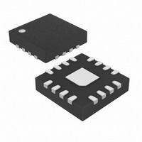
MAX7302ATE+T Maxim Integrated Products, MAX7302ATE+T Datasheet - Page 15

MAX7302ATE+T
Manufacturer Part Number
MAX7302ATE+T
Description
IC LED DRIVER LINEAR 16-TQFN
Manufacturer
Maxim Integrated Products
Type
Linear (I²C Interface)r
Datasheet
1.MAX7302AEE.pdf
(30 pages)
Specifications of MAX7302ATE+T
Topology
Open Drain, PWM
Number Of Outputs
9
Internal Driver
Yes
Type - Primary
Backlight, LED Blinker
Type - Secondary
White LED
Frequency
1MHz
Voltage - Supply
1.62 V ~ 3.6 V
Mounting Type
Surface Mount
Package / Case
16-TQFN Exposed Pad
Operating Temperature
-40°C ~ 125°C
Current - Output / Channel
25mA
Internal Switch(s)
Yes
Lead Free Status / RoHS Status
Lead free / RoHS Compliant
Voltage - Output
-
Efficiency
-
Lead Free Status / Rohs Status
Details
function to synchronize multiple MAX7302s that are oper-
ating from the same OSCIN, or to synchronize a single
MAX7302’s blink timing to an external event. Configure
the RST input to reset the internal timing counters used by
PWM and blink by setting bit D1 of the device configura-
tion register 0x26 (see Table 3).
The MAX7302 uses the internal oscillator by default.
Configure port P2 using device configuration register
0x27 bit D2 (see Table 4) as an external clock source
input, OSCIN, if the application requires a particular or
more accurate timing for the PWM or blink functions.
OSCIN only applies to PWM and blink; the MAX7302
always uses the internal oscillator for debouncing and
bus timeout. OSCIN can range up to 1MHz. Use device
configuration register 0x27 bit D3 (see Table 4) to con-
figure port P3 as OSCOUT to output a MAX7302’s
clock. The MAX7302 buffers the clock output of either
the internal oscillator OSC or the external clock source
OSCIN, according to port D2’s setup. Synchronize mul-
tiple MAX7302s without using an external clock source
input by configuring one MAX7302 to generate
Figure 5. Synchronizing Multiple MAX7302s (External Clock)
Table 9. PWM Settings on Output Port
Port P_ is a static logic-level low output port
Port P_ is a PWM output port; PWM duty cycle is 1/32
Port P_ is a PWM output port; PWM duty cycle is 2/32
Port P_ is a PWM output port; PWM duty cycle is 3/32
Port P_ is a PWM output port; PWM duty cycle is 4/32
Port P_ is a PWM output port; PWM duty cycle is 30/32
Port P_ is a PWM output port; PWM duty cycle is 31/32
Port P_ is a static logic-level high output port
Level-Translating GPIO and LED Driver with CLA
OSCILLATOR
OSCILLATOR
EXTERNAL
EXTERNAL
PWM SETTINGS
______________________________________________________________________________________
0 TO 1MHz
0 TO 1MHz
…
P2/OSCIN
P2/OSCIN
MAX7302
MAX7302
P3/OSCOUT
SMBus/I
D7
0
0
0
0
0
0
0
0
OSCOUT from its internal clock, and use this signal to
drive the remaining MAX7302s’ OSCIN.
A PWM period contains 32 cycles of the nominal 1kHz
PWM clock (see Figure 6). Set ports individually to a
PWM duty cycle between 0/32 and 31/32. For static
logic-level low output, set the ports to 0/32 PWM, and
for static logic-level high output, set the port register to
0111XXXX (see Table 9). The MAX7302 staggers the
PWM timing of the 9-port outputs, in single or dual
ports, by 1/8 of the PWM period. These phase shifts
distribute the port-output switching points across the
PWM period (see Figure 7). This staggering reduces
the di/dt output-switching transient on the supply and
also reduces the peak/mean current requirement.
All ports feature LED blink control. A global blink period
of 1/8s, 1/4s, 1/2s, 1s, 2s, 4s, or 8s applies to all ports
(see Table 10). Any port can blink during this period
with a 1/16 to 15/16 duty cycle, adjustable in 1/16
increments (see Table 11). For PWM fan control, the
MAX7302 can set the blink frequency to 32Hz.
P2/OSCIN
P2/OSCIN
D6
X
X
X
X
X
X
X
1
2
MAX7302
MAX7302
C Interfaced 9-Port,
D5
0
0
0
0
0
0
0
1
P3/OSCOUT
REGISTER DATA
D4
0
0
0
0
0
1
1
1
…
D3
X
0
0
0
0
0
1
1
P2/OSCIN
P2/OSCIN
D2
0
0
0
0
1
1
1
X
MAX7302
MAX7302
D1
X
0
0
1
1
0
1
1
D0
X
0
1
0
1
0
0
1
15


