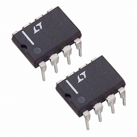
LT1166CN8 Linear Technology, LT1166CN8 Datasheet - Page 12

LT1166CN8
Manufacturer Part Number
LT1166CN8
Description
IC BIAS SYS AUTO PWR-OUTPUT 8DIP
Manufacturer
Linear Technology
Datasheet
1.LT1166CN8.pdf
(16 pages)
Specifications of LT1166CN8
Configuration
High and Low Side, Synchronous
Input Type
Non-Inverting
Delay Time
250ns
Number Of Configurations
1
Number Of Outputs
2
Operating Temperature
0°C ~ 70°C
Mounting Type
Through Hole
Package / Case
8-DIP (0.300", 7.62mm)
Lead Free Status / RoHS Status
Contains lead / RoHS non-compliant
Voltage - Supply
-
Current - Peak
-
High Side Voltage - Max (bootstrap)
-
Available stocks
Company
Part Number
Manufacturer
Quantity
Price
Part Number:
LT1166CN8
Manufacturer:
LTNEAR
Quantity:
20 000
APPLICATIONS
LT1166
100W Audio Power Amplifier
The details of a low distortion audio amplifier are shown in
Figure 19. The LT1360, designated U1, was chosen for its
good CMRR and is operated in suspended-supply mode at
a closed-loop gain of – 26.5V/V. The 15V supplies of U1
are effectively bootstrapped by the output at point D and
are generated as shown in Figure 14. A 3V
will cause an 80V
the gain of – 26.5V/V of U1, while C1 compensates for the
additional pole generated by the CMRR of U1. The rest of
the circuit (point A to point D) is an ultralow distortion
unity-gain buffer.
The main component in the unity-gain buffer is U4
(LT1166). This controller performs two important func-
tions, first it modifies the DC voltage between the gates of
M1 and M2 by keeping the product of the voltage across
R20 and R21 constant. Its secondary role is to perform
current limit, protecting M1 and M2 during short circuit.
12
Figure 15. 0.3% THD at 10kHz, P
Figure 16. Clipping at 1kHz, R
PP
U
output at point A. Resistors 7 to 10 set
INFORMATION
U
O
W
= 350W, R
L
= 8
P-P
1166 • F15
1166 • F16
signal at V
L
U
= 8
IN
The function of U3 is to drive the gates of M1 and M2. This
amplifier’s real output is not point C as it appears, but
rather the Power Supply pins. Current through R6 is used
to modulate the supply current and thus provide drive to
V
(through its supply pins) is very high, it is not able to drive
the capacitive inputs of M1 and M2 with the combination
of speed and accuracy needed to have very low distortion
at 20kHz. The purposes of U2 are to drive the gate
capacitance of M1 and M2 through its low output imped-
ance and to reduce the nonlinearty of the M1 and M2
transconductance. R24, C4 set a frequency above which
U2 no longer looks after U3 and U4, but just looks after
itself as its gain goes through unity. R1/R2 and C2/C3 are
compensation components for the CMRR feedthough.
Curves showing the performance of the amplifier are
shown in Figures 20 through 22.
TOP
and V
BOTTOM
Figure 17. 2kHz Square-Wave, C
0.01
0.1
1.0
10
Figure 18. THD vs Frequency
P
R
O
L
. Because the output impedance of U3
= 350W
= 8
100
FREQUENCY (Hz)
1k
10k
L
LT1166 • F18
= 1 F
1166 • F17
100k


