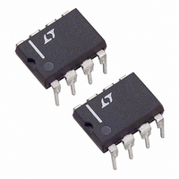
LT1166CN8 Linear Technology, LT1166CN8 Datasheet - Page 6

LT1166CN8
Manufacturer Part Number
LT1166CN8
Description
IC BIAS SYS AUTO PWR-OUTPUT 8DIP
Manufacturer
Linear Technology
Datasheet
1.LT1166CN8.pdf
(16 pages)
Specifications of LT1166CN8
Configuration
High and Low Side, Synchronous
Input Type
Non-Inverting
Delay Time
250ns
Number Of Configurations
1
Number Of Outputs
2
Operating Temperature
0°C ~ 70°C
Mounting Type
Through Hole
Package / Case
8-DIP (0.300", 7.62mm)
Lead Free Status / RoHS Status
Contains lead / RoHS non-compliant
Voltage - Supply
-
Current - Peak
-
High Side Voltage - Max (bootstrap)
-
Available stocks
Company
Part Number
Manufacturer
Quantity
Price
Part Number:
LT1166CN8
Manufacturer:
LTNEAR
Quantity:
20 000
LT1166
APPLICATIONS
as V
R
through R
Q6. The reduced current has the effect of reducing the drop
on R
The open-loop voltage gain V
increased by replacing R
The effect of this is to increase the voltage gain V
from approximately 0.8 to 1 (see Typical Performance
Characteristics curves). The use of current sources in-
stead of resistors greatly increases loop gain and this
compensates for the nonlinearity of the output stage
resulting in much lower distortion.
Frequency Compensation and Stability
The input transconductance is set by the input resistor R
and the 32:1 current mirrors Q3/Q4 and Q5/Q6. The
resistors R1 and R2 are small compared to the value of
R
which drive external compensation capacitors C
C
give an input transconductance of:
The gain bandwidth is:
Depending on the speed of the output devices, typical
values are R
– 3dB bandwidth of 1.2MHz (see Typical Performance
Characteristics curves).
To prevent instability it is important to provide good
supply bypassing as shown in Figure 1. Large supply
bypass capacitors (220 F) and short power leads can
eliminate instabilities at these high current levels. The
100 resistors (R2 and R3) in series with the gates of the
output devices stop oscillations in the 100MHz region as do
the 100 resistors R1 and R4 in Figure 1.
6
EXT2
IN
IN
g
GBW =
, current that was flowing in R1 and Q1 is now supplied
. Current in R
m
IN
T
. These two input signal paths appear in parallel to
, and V
. Similarly for V
= 16/R
IN
2 (R
. This effect reduces the current in mirror Q5/
IN
T
IN
rises to make V
= 4.3k and C
IN
IN
16
)(C
U
appears 32 times larger in Q4 or Q6,
T
EXT
, when positive voltage is applied to
INFORMATION
T
)
U
and R
EXT1
O
track V
O
= C
B
/(V
with current sources.
EXT2
W
IN
IN
– V
= 500pF giving a
.
PIN2
U
) can be
EXT1
OUT
/ V
and
IN
IN
Driving Capacitive Loads
Ideally, amplifiers have enough phase margin that they
don’t oscillate but just slow down with capacitive loads.
Practically, amplifiers that drive significant power require
some isolation from heavy capacitive loads to prevent
oscillation. This isolation is normally an inductor in series
with the output of the amplifier. A 1 H inductor in parallel
with a 10 resistor is sufficient for many applications.
Setting Output AB Bias Current
Setting the output AB quiescent current requires no ad-
justments. The internal op amps force V
between each Sense (Pins 5 and 8) to the Output (Pin 3).
At quiescent levels the output current is set by:
The LT1166 does not require a heat sink or mounting on
the heat sink for thermal tracking. The temperature coef-
ficient of V
junction temperature of the LT1166 and not the tempera-
ture of the power transistors.
Output Offset Voltage and Input Bias Current
The output offset voltage is a function of the value of R
and the mismatch between external current sources I
and I
curves). Any error in I
by the 32:1 input current mirror, but is multiplied by the
input resistor R
Current Limit
The voltage to activate the current limit is 1.3V. The
simplest way to protect the output transistors is to con-
nect the Current Limit pins 6 and 7 to the Sense pins 5 and
8. A current limit of 1.3A can be set by using 1 sense
resistors. To keep the current limit circuit from oscillating
in hard limit, it is necessary to add an RC (1k and 1 F)
between the Sense pin and the I
or decrease the current limit without changing AB bias
current in the power transistors. Figure 4 demonstrates
The sense resistors can be tapped up or down to increase
I
AB
BOTTOM
= 20mV/R
AB
(see the Typical Performance Characteristics
is approximately 0.3%/ C and is set by the
IN
SENSE
.
TOP
and I
BOTTOM
LIM
as shown in Figure 1.
match is reduced
AB
= 20mV
TOP
IN


