BTS555 Infineon Technologies, BTS555 Datasheet - Page 2
BTS555
Manufacturer Part Number
BTS555
Description
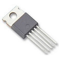
IC HISIDE PWR SWTCH TO218AB/5-1
Manufacturer
Infineon Technologies
Series
PROFET®r
Type
High Sider
Specifications of BTS555
Input Type
Non-Inverting
Number Of Outputs
1
On-state Resistance
1.9 mOhm
Current - Output / Channel
165A
Current - Peak Output
520A
Voltage - Supply
5 V ~ 34 V
Operating Temperature
-40°C ~ 150°C
Mounting Type
Through Hole
Package / Case
TO-218AB/5
Module Configuration
High Side
Peak Output Current
165A
Output Resistance
1.9ohm
Input Delay
600µs
Output Delay
200µs
Supply Voltage Range
5V To 34V
Driver Case Style
TO-218AB
No. Of Pins
5
Operating Temperature Range
-40°C To +150°C
Rohs Compliant
No
Device Type
High Side
Lead Free Status / RoHS Status
Contains lead / RoHS non-compliant
Other names
BTS555NK
SP000011266
SP000011266
Available stocks
Company
Part Number
Manufacturer
Quantity
Price
Company:

Part Number:
BTS555
Manufacturer:
INFINEON
Quantity:
3 000
Part Number:
BTS555
Manufacturer:
INFINEON/英飞凌
Quantity:
20 000
Company:
Part Number:
BTS555E3146HKSA1
Manufacturer:
INFINEON
Quantity:
12 000


Maximum Ratings at T
Parameter
Supply voltage (overvoltage protection see page 4)
Supply voltage for full short circuit protection,
(E
Load current (short circuit current, see page 5)
Load dump protection V
Operating temperature range
Storage temperature range
Power dissipation (DC), T
Inductive load switch-off energy dissipation, single pulse
Electrostatic discharge capability (ESD)
Current through input pin (DC)
Current through current sense status pin (DC)
4)
5)
6)
7)
Infineon Technologies AG
see internal circuit diagrams on page 7 and 8
R
IN, IS = open or grounded
V
I
Pin
Human Body Model acc. MIL-STD883D, method 3015.7 and ESD
assn. std. S5.1-1993, C = 100 pF, R = 1.5 k
AS
L
bb
I
= 20 A, Z
6
Not shorting all outputs will considerably increase the on-state resistance, reduce the peak current capability
and decrease the current sense accuracy
Otherwise add up to 0.5 m (depending on used length of the pin) to the R
tab.
R
V
limitation see diagram on page 9)
)
1
2
3
4
5
Load dump
= 2 , R
I
= 12V, T
= internal resistance of the load dump test pulse generator.
L
is setup without the DUT connected to the generator per ISO 7637-1 and DIN 40839.
L
j,start
Symbol
= 15 mH, 0 ,
= 0.1 , t
OUT
OUT
V bb
IN
IS
= 150°C, T
d
LoadDump
= 200 ms,
j
O
+
O
S
= 25 °C unless otherwise specified
I
C
see diagrams on page 10
C
25 °C
= 150°C const.,
Function
Output to the load. The pins 1 and 5 must be shorted with each other
especially in high current applications!
Input, activates the power switch in case of short to ground
Positive power supply voltage, the tab is electrically connected to this pin.
In high current applications the tab should be used for the V
instead of this pin
Diagnostic feedback providing a sense current proportional to the load
current; zero current on failure (see Truth Table on page 7)
Output to the load. The pins 1 and 5 must be shorted with each other
especially in high current applications!
= U
A
T
+ V
j,start
s
, U
=-40 .+150°C:
A
5 )
2
= 13.5 V
.
V
V
I
V
T
T
P
E
V
I
I
Symbol
L
IN
IS
j
stg
Load dump
bb
bb
tot
AS
ESD
4 )
4)
ON
7
if the pin is used instead of the
)
Data Sheet BTS555
-40 ...+150
-55 ...+150
self-limited
+15 , -250
+15 , -250
Values
2008-June-24
bb
360
connection
4.0
40
34
80
3
Unit
mA
kV
°C
W
V
V
A
V
J
Related parts for BTS555
Image
Part Number
Description
Manufacturer
Datasheet
Request
R

Part Number:
Description:
Manufacturer:
Infineon Technologies AG
Datasheet:
Part Number:
Description:
Manufacturer:
Infineon Technologies AG
Datasheet:
Part Number:
Description:
Manufacturer:
Infineon Technologies AG
Datasheet:
Part Number:
Description:
Manufacturer:
Infineon Technologies AG
Datasheet:
Part Number:
Description:
Manufacturer:
Infineon Technologies AG
Datasheet:
Part Number:
Description:
Manufacturer:
Infineon Technologies AG
Datasheet:
Part Number:
Description:
Manufacturer:
Infineon Technologies AG
Datasheet:
Part Number:
Description:
16-bit microcontroller with 2x2 KByte RAM
Manufacturer:
Infineon Technologies AG
Datasheet:
Part Number:
Description:
NPN silicon RF transistor
Manufacturer:
Infineon Technologies AG
Datasheet:
Part Number:
Description:
NPN silicon RF transistor
Manufacturer:
Infineon Technologies AG
Datasheet:
Part Number:
Description:
NPN silicon RF transistor
Manufacturer:
Infineon Technologies AG
Datasheet:
Part Number:
Description:
NPN silicon RF transistor
Manufacturer:
Infineon Technologies AG
Datasheet:
Part Number:
Description:
Si-MMIC-amplifier in SIEGET 25-technologie
Manufacturer:
Infineon Technologies AG
Datasheet:
Part Number:
Description:
IGBT Power Module
Manufacturer:
Infineon Technologies AG
Datasheet:
Part Number:
Description:
IC for switching-mode power supplies
Manufacturer:
Infineon Technologies AG
Datasheet: