BTS555 Infineon Technologies, BTS555 Datasheet - Page 5
BTS555
Manufacturer Part Number
BTS555
Description
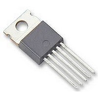
IC HISIDE PWR SWTCH TO218AB/5-1
Manufacturer
Infineon Technologies
Series
PROFET®r
Type
High Sider
Specifications of BTS555
Input Type
Non-Inverting
Number Of Outputs
1
On-state Resistance
1.9 mOhm
Current - Output / Channel
165A
Current - Peak Output
520A
Voltage - Supply
5 V ~ 34 V
Operating Temperature
-40°C ~ 150°C
Mounting Type
Through Hole
Package / Case
TO-218AB/5
Module Configuration
High Side
Peak Output Current
165A
Output Resistance
1.9ohm
Input Delay
600µs
Output Delay
200µs
Supply Voltage Range
5V To 34V
Driver Case Style
TO-218AB
No. Of Pins
5
Operating Temperature Range
-40°C To +150°C
Rohs Compliant
No
Device Type
High Side
Lead Free Status / RoHS Status
Contains lead / RoHS non-compliant
Other names
BTS555NK
SP000011266
SP000011266
Available stocks
Company
Part Number
Manufacturer
Quantity
Price
Company:

Part Number:
BTS555
Manufacturer:
INFINEON
Quantity:
3 000
Part Number:
BTS555
Manufacturer:
INFINEON/英飞凌
Quantity:
20 000
Company:
Part Number:
BTS555E3146HKSA1
Manufacturer:
INFINEON
Quantity:
12 000


Parameter and Conditions
at T
Protection Functions
Short circuit current limit
Short circuit shutdown delay after input current
positive slope, V
min. value valid only if input "off-signal" time exceeds 30 s
Output clamp
(inductive load switch off)
Output clamp (inductive load switch off)
Short circuit shutdown detection voltage
Thermal overload trip temperature
Thermal hysteresis
Reverse Battery
Reverse battery voltage
On-state resistance
Integrated resistor in V
16
17
18
19
Infineon Technologies AG
V
I
V
at V
(pin 3 to pins 1,5)
L
) Integrated protection functions are designed to prevent IC destruction under fault conditions described in the
) This output clamp can be "switched off" by using an additional diode at the IS-Pin (see page 8). If the diode
) The reverse load current through the intrinsic drain-source diode has to be limited by the connected load (as
bb
) Short circuit is a failure mode. The device is not designed to operate continuously into a short circuit by
= 40 mA
ON
j
data sheet. Fault conditions are considered as “outside” normal operating range. Protection functions are not
designed for continuous repetitive operation.
permanent resetting the short circuit latch function. The lifetime will be reduced under such conditions.
is used, V
it is done with all polarity symmetric loads). Note that under off-conditions (I
is not activated. This results in raised power dissipation due to the higher voltage drop across the intrinsic
drain-source diode. The temperature protection is not active during reverse current operation! Increasing
reverse battery voltage capability is simply possible as described on page 9.
= -40 ... +150 °C, V
= -12V, V
= 12 V, time until shutdown max. 300 s
OUT
= V
OUT
bb
IN
18
- V
= 0, I
is clamped to V
)
ON
ON(CL)
> V
bb
L
(Pins 1,5 to pin 3)
= - 30 A, R
= 12 V unless otherwise specified
16
ON(SC)
bb
(e.g. overvoltage)
)
19
(Tab to pins 1,5)
line
)
bb
- V
IS
ON(CL)
= 1 k
at inductive load switch off.
T
17
c
T
I
T
T
)
L
j
T
T
j
=+150°C:
T
c
= 40 mA:
= 150 °C:
j
= 150 °C:
c
j
= 25 °C:
=-40°C:
= 25 °C:
=25°C:
5
I
t
-V
V
V
T
-V
R
R
Symbol
L(SCp)
d(SC)
jt
T
ON(CL)
ON(SC)
ON(rev)
bb
OUT(CL)
bb
jt
1)
IN
200
200
300
150
105
min
80
14
40
90
= I
--
--
--
--
Data Sheet BTS555
IS
= 0) the power transistor
Values
320
400
480
110
125
2.3
3.9
typ
17
44
10
--
--
--
6
2008-June-24
max
550
620
650
300
135
150
3.0
4.7
20
47
16
--
--
--
Unit
m
°C
A
V
V
V
K
V
s
Related parts for BTS555
Image
Part Number
Description
Manufacturer
Datasheet
Request
R

Part Number:
Description:
Manufacturer:
Infineon Technologies AG
Datasheet:
Part Number:
Description:
Manufacturer:
Infineon Technologies AG
Datasheet:
Part Number:
Description:
Manufacturer:
Infineon Technologies AG
Datasheet:
Part Number:
Description:
Manufacturer:
Infineon Technologies AG
Datasheet:
Part Number:
Description:
Manufacturer:
Infineon Technologies AG
Datasheet:
Part Number:
Description:
Manufacturer:
Infineon Technologies AG
Datasheet:
Part Number:
Description:
Manufacturer:
Infineon Technologies AG
Datasheet:
Part Number:
Description:
16-bit microcontroller with 2x2 KByte RAM
Manufacturer:
Infineon Technologies AG
Datasheet:
Part Number:
Description:
NPN silicon RF transistor
Manufacturer:
Infineon Technologies AG
Datasheet:
Part Number:
Description:
NPN silicon RF transistor
Manufacturer:
Infineon Technologies AG
Datasheet:
Part Number:
Description:
NPN silicon RF transistor
Manufacturer:
Infineon Technologies AG
Datasheet:
Part Number:
Description:
NPN silicon RF transistor
Manufacturer:
Infineon Technologies AG
Datasheet:
Part Number:
Description:
Si-MMIC-amplifier in SIEGET 25-technologie
Manufacturer:
Infineon Technologies AG
Datasheet:
Part Number:
Description:
IGBT Power Module
Manufacturer:
Infineon Technologies AG
Datasheet:
Part Number:
Description:
IC for switching-mode power supplies
Manufacturer:
Infineon Technologies AG
Datasheet: