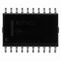
NCP1652DWR2G ON Semiconductor, NCP1652DWR2G Datasheet - Page 20

NCP1652DWR2G
Manufacturer Part Number
NCP1652DWR2G
Description
IC PFC CONTROLLER CCM/DCM 20SOIC
Manufacturer
ON Semiconductor
Datasheet
1.NCP1652DR2G.pdf
(34 pages)
Specifications of NCP1652DWR2G
Mode
Continuous Conduction (CCM), Discontinuous Conduction (DCM)
Frequency - Switching
100kHz
Current - Startup
5.62mA
Voltage - Supply
9.3 V ~ 20 V
Operating Temperature
-40°C ~ 125°C
Mounting Type
Surface Mount
Package / Case
20-SOIC (7.5mm Width)
Switching Frequency
20 KHz to 250 KHz
Maximum Operating Temperature
+ 125 C
Mounting Style
SMD/SMT
Minimum Operating Temperature
- 40 C
Lead Free Status / RoHS Status
Lead free / RoHS Compliant
Other names
NCP1652DWR2GOSTR
main switch, a resistor−capacitor−diode (RCD) clamp, a
transient voltage suppressor (TVS) or an active clamp using
a MOSFET and capacitor can be used as shown in
Figures 54 to 56.
V
V
There are a few methods to clamp the voltage spike on the
the 2−stage solution. As a result, potentially higher
leakage inductance induces higher voltage spikes (like
the one shown in Figure 53) on the MOSFET drain.
This may require a MOSFET with a higher voltage
rating compared to similar dc−input flyback
applications.
in
in
Figure 53. Typical Drain Voltage Waveform of a
R
TVS
C
Figure 54. RCD Clamp
Figure 55. TVS Clamp
Flyback Main Switch
D
RCD
Clamp
TVS
Clamp
http://onsemi.com
V
V
out
out
20
energy in the clamping circuits – the dissipation is
proportional to LI
transformer and I is the peak of the switch current at
turn−off. An RDC snubber is simple and has the lowest cost,
but constantly dissipates power. A TVS provides good
voltage clamping at a slightly higher cost and dissipates
power only when the drain voltage exceeds the voltage
rating of the TVS.
to the other methods. It requires addition of a MOSFET and
a high voltage capacitor as part of the active clamp circuit,
thus adding complexity, but it results in a complete reuse of
the leakage inductance energy. As a result, the transformer
construction is no longer critical and one can use cheaper
cost solution. Also, the active clamp circuit reduces the
voltage stress on the primary switch and that can lead to
usage of lower cost or lower on resistance (R
MOSFET. Finally, the turn−on switching losses are
eliminated because the active clamp circuit allows the
discharge of the MOSFET C
turn−on. The energy stored in the leakage inductance is
utilized for this transition.
clamp circuit may not be justified. However, the OUTB of
the NCP1652 is also usable for another purpose,
synchronous
rectification for flyback converters is an emerging
requirement for flyback converters. The OUTB signal from
NCP1652 is ideal for interfacing with a secondary side
synchronous rectifier controller such as NCP4303 as shown
in Figure 57. As shown in Figure 57, using the OUTB
(coupled through pulse transformer or Y−capacitor) as a
trigger for the NCP4303 allows guaranteed turn−off of the
secondary side synchronous MOSFET prior to turn−on of
the primary switch. In any CCM flyback converter, this is a
critical requirement to prevent cross−conduction and
NCP1652 and NCP4303 combination is the first such
chipset
cross−conduction.
V
The first two methods result in dissipation of the leakage
The active clamp circuit provides an intriguing alternative
In many applications, the added complexity of the active
in
that
Figure 56. Active Clamp
rectification
2
guarantees
where L is the leakage inductance of the
Active
Clamp
OSS
the
control.
capacitance prior to the
operation
Synchronous
without
DS(on)
V
out
)


