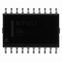
NCP1652DWR2G ON Semiconductor, NCP1652DWR2G Datasheet - Page 23

NCP1652DWR2G
Manufacturer Part Number
NCP1652DWR2G
Description
IC PFC CONTROLLER CCM/DCM 20SOIC
Manufacturer
ON Semiconductor
Datasheet
1.NCP1652DR2G.pdf
(34 pages)
Specifications of NCP1652DWR2G
Mode
Continuous Conduction (CCM), Discontinuous Conduction (DCM)
Frequency - Switching
100kHz
Current - Startup
5.62mA
Voltage - Supply
9.3 V ~ 20 V
Operating Temperature
-40°C ~ 125°C
Mounting Type
Surface Mount
Package / Case
20-SOIC (7.5mm Width)
Switching Frequency
20 KHz to 250 KHz
Maximum Operating Temperature
+ 125 C
Mounting Style
SMD/SMT
Minimum Operating Temperature
- 40 C
Lead Free Status / RoHS Status
Lead free / RoHS Compliant
Other names
NCP1652DWR2GOSTR
Power dissipation should be controlled to avoid exceeding
the maximum power dissipation of the controller. If
dissipation on the controller is excessive, a resistor can be
placed in series with the HV pin. This will reduce power
dissipation on the controller and transfer it to the series
resistor.
Drive Outputs
adjustable non−overlap delay (t
drives the primary MOSFET. The secondary output, OUTB,
is designed to provide a logic signal used to control a
synchronous rectification switch in the secondary side, an
active clamp switch in the primary or both. The outputs are
biased directly from V
approximately V
resistance of 8.0 W (typical) OUTB has a source resistance
22 W (typical) and a sink resistance of 10 W (typical). OUTB
is a purposely sized smaller than OUTA because the gate
charge of an active switch or logic used with synchronous
rectification is usually less than that of the primary
MOSFET. If a higher drive capability is required, an external
discrete driver can be used.
there are no faults present. They are disabled once V
discharges to V
generated when the outputs are disabled due to a fault
(latch−off, V
terminates at the end of the clock cycle. This ensures the
active clamp capacitor is reset.
may generate voltage spikes during switch transitions due to
parasitic board inductance. Shortening the connection
length between the drivers and their loads and using wider
connections will reduce inductance−induce spikes.
The startup circuit is rated at a maximum voltage of 500 V.
The NCP1652 has out off phase output drivers with an
OUTA has a source resistance of 13 W (typical) and a sink
The drivers are enabled once V
The high current drive capability of OUTA and OUTB
CC(off)
V
CC
CC(off)
IN
, overload, or brown−out). The last pulse
.
. OUTB is always the last pulse
CC
and their high state voltage is
D
). The main output, OUTA,
CC
reaches V
CC(on)
Figure 60. Peak charger
http://onsemi.com
Peak Charger
and
CC
NCP1652
23
HV
Adjustable Dead Time
transitions to prevent simultaneous conduction of the main
and synchronous rectifier or active clamp MOSFETs. The
delay is also used to optimize the turn−off transition of the
active clamp switch to achieve zero−volt switching of the
main switch in an active clamp topology. Figure 61 shows
the timing relationship between OUTA and OUTB.
connecting a resistor, R
overlap delay is proportional to R
set between 80 ns and 1.8 ms using the formula:
AC Error Amplifier and Buffer
a high quality sine wave by forcing the filtered input current
to follow the output of the reference generator. The output
of the reference generator is a full wave rectified ac signal
and it is applied to the non inverting input of the EA. The
filtered input current, I
OUTA
OUTA and OUTB have an adjustable dead time between
The dead time between OUTA and OUTB is adjusted by
The AC error amplifier (EA) shapes the input current into
Figure 61. Timing relationship between OUTA and
t
delay
t
delay
(in ns) + 8.0
(lead)
OUTA
OUTB
R
delay
varying between 10 kW and 230 kW
in
D
R
, is the current sense signal at the
, from the R
OUTB.
delay
(in kW) with
t
delay
D
. The delay time can be
(trail)
D
V
OUT
pin to ground. The


