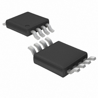
LTC1967CMS8#PBF Linear Technology, LTC1967CMS8#PBF Datasheet - Page 13

LTC1967CMS8#PBF
Manufacturer Part Number
LTC1967CMS8#PBF
Description
IC CONVERTER RMS-DC PREC 8MSOP
Manufacturer
Linear Technology
Datasheet
1.LTC1967CMS8.pdf
(28 pages)
Specifications of LTC1967CMS8#PBF
Current - Supply
320µA
Voltage - Supply
5.0V
Mounting Type
Surface Mount
Package / Case
8-MSOP, Micro8™, 8-uMAX, 8-uSOP,
Lead Free Status / RoHS Status
Lead free / RoHS compliant by exemption
Available stocks
Company
Part Number
Manufacturer
Quantity
Price
APPLICATIO S I FOR ATIO
Output Connections
The LTC1967 output is differentially, but not symmetri-
cally, generated. That is to say, the RMS value that the
LTC1967 computes will be generated on the output (Pin 5)
relative to the output return (Pin 6), but these two pins are
not interchangeable. For most applications, Pin 6 will be
tied to ground (Pin 1). However, Pin 6 can be tied to any
voltage between 0V and V
output voltage swing desired. This last restriction keeps
V
reference level other than ground is used, it should be a
low impedance, both AC and DC, for proper operation of
the LTC1967.
In any configuration, the averaging capacitor should be
connected between Pins 5 and 6. The LTC1967 RMS-DC
output will be a positive voltage created at V
with respect to OUT RTN (Pin 6).
Power Supply Bypassing
The LTC1967 is a switched capacitor device, and large
transient power supply currents will be drawn as the
switching occurs. For reliable operation, standard power
supply bypassing must be included. A 0.01 F capacitor
from V
will suffice. If there is a good quality ground plane avail-
able, the capacitors can go directly to that instead. Power
supply bypass capacitors can, of course, be inexpensive
ceramic types.
Up and Running!
If you have followed along this far, you should have the
LTC1967 up and running by now! Don’t forget to enable
the device by grounding Pin 8, or driving it with a logic low.
Keep in mind that the LTC1967 output impedance is fairly
high, and that even the standard 10M input impedance
of a digital multimeter (DMM) or a 10 scope probe will load
down the output enough to degrade its typical gain error
of 0.1%. In the end application circuit, either a buffer or
another component with an extremely high input imped-
ance (such as a dual slope integrating ADC) should be used.
OUT
itself (Pin 5) within the range of 0V to V
+
(Pin 7) to GND (Pin 1) located close to the device
U
U
+
(Pin 7) less the maximum
W
OUT
U
(Pin 5)
+
. If a
For laboratory evaluation, it may suffice to use a bench-top
DMM with the ability to disconnect the 10M shunt.
If you are still having trouble, it may be helpful to skip
ahead a few pages and review the Troubleshooting Guide.
What About Response Time?
With a large value averaging capacitor, the LTC1967 can
easily perform RMS-to-DC conversion on low frequency
signals. It compares quite favorably in this regard to prior-
generation products because nothing about the
circuitry is temperature sensitive. So the RMS result
doesn’t get distorted by signal driven thermal fluctuations
like a log-antilog circuit output does.
However, using large value capacitors results in a slow
response time. Figure 10 shows the rising and falling step
responses with a 1 F averaging capacitor. Although they
both appear at first glance to be standard exponential-
decay type settling, they are not. This is due to the
nonlinear nature of an RMS-to-DC calculation. Also note
the change in the time scale between the two; the rising
edge is more than twice as fast to settle to a given
accuracy. Again this is a necessary consequence of RMS-
to-DC calculation.
Although shown with a step change between 0mV and
100mV, the same response shapes will occur with the
LTC1967 for ANY step size. This is in marked contrast to
prior generation log/antilog RMS-to-DC converters, whose
averaging time constants are dependent on the signal
level, resulting in excruciatingly long waits for the output
to go to zero.
The shape of the rising and falling edges will be dependent
on the total percent change in the step, but for less than the
100% changes shown in Figure 10, the responses will be
less distorted and more like a standard exponential decay.
For example, when the input amplitude is changed from
3
100mV. At very low frequencies, the LTC1967 will essentially track the input. But as the input
frequency is increased, the average result will converge to the RMS value of the input. If the rise and
fall characteristics were symmetrical, the output would converge to 50mV. In fact though, the RMS
value of a 100mV DC-coupled 50% duty cycle pulse train is 70.71mV, which the asymmetrical rise
and fall characteristics will converge to as the input frequency is increased.
To convince oneself of this necessity, consider a pulse train of 50% duty cycle between 0mV and
3
LTC1967
13
1967f


