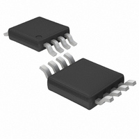
LTC1967CMS8#PBF Linear Technology, LTC1967CMS8#PBF Datasheet - Page 23

LTC1967CMS8#PBF
Manufacturer Part Number
LTC1967CMS8#PBF
Description
IC CONVERTER RMS-DC PREC 8MSOP
Manufacturer
Linear Technology
Datasheet
1.LTC1967CMS8.pdf
(28 pages)
Specifications of LTC1967CMS8#PBF
Current - Supply
320µA
Voltage - Supply
5.0V
Mounting Type
Surface Mount
Package / Case
8-MSOP, Micro8™, 8-uMAX, 8-uSOP,
Lead Free Status / RoHS Status
Lead free / RoHS compliant by exemption
Available stocks
Company
Part Number
Manufacturer
Quantity
Price
APPLICATIO S I FOR ATIO
The trade-off here is that on the one hand, the DC error is
input frequency dependent, so a calibration signal fre-
quency high enough to make the DC error negligible
should be used. On the other hand, as low a frequency as
can be used is best to avoid attenuation of the calibrated
AC signal, either from parasitic RC loading or insufficient
op amp gain. For instance, with a 1kHz calibration signal,
a 1MHz op amp will typically only have 60dB of open-loop
gain, so it could attenuate the calibration signal a full 0.1%.
AC-Only, 2 Point
The next most significant error for AC-coupled applica-
tions will be the effect of output offset voltage, noticeable
at the bottom end of the input scale. This too can be
calibrated out if two measurements are made, one with a
full-scale sine wave input and a second with a sine wave
input (of the same frequency) at 10% of full scale. The
trade-off in selecting this second level is that it should be
small enough that the gain error effect becomes small
compared to the gain error effect at full scale, while on the
other hand, not using so small an input that the input offset
voltage becomes an issue.
The calculations of the error terms for a 200mV full-scale
case are:
DC, 2 Point
DC-based calibration is preferable in many cases because
a DC voltage of known, good accuracy is easier to gener-
ate than such an AC calibration voltage. The only down
side is that the LTC1967 input offset voltage plays a role.
It is therefore suggested that a DC-based calibration
scheme check at least two points: full scale. Applying the
Gain =
Output Offset =
Reading at 200mV – Reading at 20mV
U
Reading at 20mV
U
180mV
Gain
W
– 20mV
U
–full-scale input can be done by physically inverting the
voltage or by applying the same +full-scale input to the
opposite LTC1967 input.
For an otherwise AC-coupled application, only the gain
term may be worth correcting for, but for DC-coupled
applications, the input offset voltage can also be calcu-
lated and corrected for.
The calculations of the error terms for a 200mV full-scale
case are:
Note: Calculation of and correction for input offset voltage
are the only way in which the two LTC1967 inputs (IN1,
IN2) are distinguishable from each other. The calculation
above assumes the standard definition of offset; that a
positive offset is the case of a positive voltage error inside
the device that must be corrected by applying a like
negative voltage outside. The offset is referred to which-
ever pin is driven positive for the +full-scale reading.
DC, 3 Point
One more point is needed with a DC calibration scheme to
determine output offset voltage: +10% of full scale.
The calculation of the input offset is the same as for the
2-point calibration above, while the gain and output offset
are calculated for a 200mV full-scale case as:
Gain =
Input Offset =
Gain =
Output Offset =
Reading at 200mV +Reading at – 200mV – 400mV • Gain
Reading at 200mV + Reading at – 200mV
Reading at 200mV – Reading at 20mV
Reading at – 200mV – Reading at 200mV
180mV
400mV
2
2 •Gain
LTC1967
23
1967f


