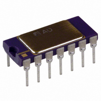
AD636KD Analog Devices Inc, AD636KD Datasheet - Page 8

AD636KD
Manufacturer Part Number
AD636KD
Description
IC TRUE RMS/DC CONV MONO 14-CDIP
Manufacturer
Analog Devices Inc
Datasheet
1.AD636JDZ.pdf
(16 pages)
Specifications of AD636KD
Rohs Status
RoHS non-compliant
Current - Supply
800µA
Voltage - Supply
±2.5 V ~ 16 V
Mounting Type
Through Hole
Package / Case
14-CDIP (0.300", 7.62mm)
Available stocks
Company
Part Number
Manufacturer
Quantity
Price
AD636
CHOOSING THE AVERAGING TIME CONSTANT
The AD636 computes the rms of both ac and dc signals. If the
input is a slowly varying dc voltage, the output of the AD636
tracks the input exactly. At higher frequencies, the average
output of the AD636 approaches the rms value of the input
signal. The actual output of the AD636 differs from the ideal
output by a dc (or average) error and some amount of ripple, as
demonstrated in
The dc error is dependent on the input signal frequency and the
value of C
value of C
frequency using the standard rms connection.
The ac component of the output signal is the ripple. There are
two ways to reduce the ripple. The first method involves using a
large value of C
to C
reduction in ripple. When measuring waveforms with high crest
factors (such as low duty cycle pulse trains), the averaging time
constant should be at least ten times the signal period. For example,
a 100 Hz pulse rate requires a 100 ms time constant, which
corresponds to a 4 μF capacitor (time constant = 25 ms per μF).
1kΩ TO 10kΩ
V
IN
NONPOLARIZED
AV
V
, a tenfold increase in this capacitance effects a tenfold
3.3µF
OUT
C2
R
Figure 7. Typical Output Waveform for Sinusoidal Input
L
AV
AV,
E
O
. Figure 8 can be used to determine the minimum
which yields a given % dc error above a given
BUF OUT
DOUBLE-FREQUENCY
RIPPLE
BUF IN
AV
Figure 7.
. Because the ripple is inversely proportional
C
Figure 6. Single-Supply Connection
–V
V
NC
dB
AV
IN
S
1
2
3
4
5
6
7
IDEAL
E
O
AD636
NC = NO CONNECT
– BUF
+
10kΩ
ABSOLUTE
DC ERROR = E
SQUARER
CURRENT
DIVIDER
MIRROR
VALUE
–
C
AV
AVERAGE E
+
10kΩ
O
– E
14
13
12
11
10
+V
9
8
O
O
= E
S
NC
NC
NC
TIME
COM
R
I
OUT
(IDEAL)
L
O
0.1µF
20kΩ
39kΩ
0.1µF
Rev. D | Page 8 of 16
The primary disadvantage in using a large C
is that the settling time for a step change in input level is
increased proportionately.
between C
of C
as for increasing signals (the values in Figure 8 are for decreasing
signals). Settling time also increases for low signal levels, as
shown in Figure 9.
A better method for reducing output ripple is the use of a post-
filter. Figure 10 shows a suggested circuit. If a single-pole filter
is used (C3 removed, R
5 times the value of C
Figure 11, and the settling time is increased. For example, with
C
reduced from 10% of reading to approximately 0.3% of reading.
The settling time, however, is increased by approximately a
factor of 3. The values of C
to permit faster settling times while still providing substantial
ripple reduction.
AV
0.01
100
0.1
10
= 1 μF and C2 = 4.7 μF, the ripple for a 60 Hz input is
AV
1
Figure 8. Error/Settling Time Graph for Use with the Standard RMS
1
. The settling time is twice as great for decreasing signals
10.0
VALUES FOR C
1% SETTLING TIME FOR
STATED % OF READING
AVERAGING ERROR*
ACCURACY ±20% DUE TO
COMPONENT TOLERANCE
*% dc ERROR + % RIPPLE (PEAK)
7.5
5.0
2.5
1.0
1mV
0
AV
and 1% settling time is 115 ms for each microfarad
10
Figure 9. Settling Time vs. Input Level
AV
INPUT FREQUENCY (Hz)
AND
AV
X
, the ripple is reduced, as shown in
100
10mV
shorted), and C2 is approximately
Figure 8 shows the relationship
AV
Connection
rms INPUT LEVEL
and C2 can therefore be reduced
1k
100mV
10k
AV
to remove ripple
100k
100
10
1
0.1
0.01
1V


