LM81BIMT-3/NOPB National Semiconductor, LM81BIMT-3/NOPB Datasheet - Page 9
LM81BIMT-3/NOPB
Manufacturer Part Number
LM81BIMT-3/NOPB
Description
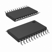
IC MONITOR SYS HARDWARE 24TSSOP
Manufacturer
National Semiconductor
Datasheet
1.LM81CIMT-3NOPB.pdf
(33 pages)
Specifications of LM81BIMT-3/NOPB
Function
Hardware Monitor
Topology
ADC (Sigma Delta), Comparator, Fan Speed Control, Register Bank
Sensor Type
External & Internal
Sensing Temperature
-40°C ~ 125°C, External Sensor
Output Type
SMBus™
Output Alarm
No
Output Fan
No
Voltage - Supply
2.8 V ~ 3.8 V
Operating Temperature
-40°C ~ 125°C
Mounting Type
Surface Mount
Package / Case
24-TSSOP
Monitored Voltage
2.5 V , 3.3 V , 5 V , 12 V
Manual Reset
Not Resettable
Watchdog
Watchdog
Battery Backup Switching
No
Supply Voltage (max)
3.8 V
Supply Voltage (min)
2.8 V
Supply Current (typ)
400 uA (Typ)
Maximum Operating Temperature
+ 125 C
Minimum Operating Temperature
- 40 C
Power Fail Detection
No
Lead Free Status / RoHS Status
Lead free / RoHS Compliant
Other names
*LM81BIMT-3
*LM81BIMT-3/NOPB
LM81BIMT-3
*LM81BIMT-3/NOPB
LM81BIMT-3
Available stocks
Company
Part Number
Manufacturer
Quantity
Price
Company:

Part Number:
LM81BIMT-3/NOPB
Manufacturer:
CYPRESS
Quantity:
169
Part Number:
LM81BIMT-3/NOPB
Manufacturer:
NS/国半
Quantity:
20 000


INT
CI
FAN1–FAN2
SMBCLK
SMBData
RESET
A0/NTEST_OUT
A1
AC Electrical Characteristics
Note 1: Absolute Maximum Ratings indicate limits beyond which damage to the device may occur. Operating Ratings indicate conditions for which the device is
functional, but do not guarantee specific performance limits. For guaranteed specifications and test conditions, see the Electrical Characteristics. The guaranteed
specifications apply only for the test conditions listed. Some performance characteristics may degrade when the device is not operated under the listed test
conditions.
Note 2: All voltages are measured with respect to GND, unless otherwise specified.
Note 3: The Absolute maximum input range for :
Note 4: When the input voltage (V
maximum package input current rating limits the number of pins that can safely exceed the power supplies with an input current of 5 mA to four.
Note 5: The maximum power dissipation must be derated at elevated temperatures and is dictated by T
allowable power dissipation at any temperature is P
Note 6: The human body model is a 100 pF capacitor discharged through a 1.5 k
directly into each pin.
Note 7: See the section titled “Surface Mount” found in any post 1986 National Semiconductor Linear Data Book for other methods of soldering surface mount
devices.
Note 8: Parasitics and or ESD protection circuitry are shown in the figure below for the LM81’s pins. The nominal breakdown voltage of the zener D3 is 6.5V. Care
should be taken not to forward bias the parasitic diode, D1, present on pins: A0/NTEST_OUT, A1 and DACOut/NTEST_IN. Doing so by more than 50 mV may corrupt
a temperature or voltage measurement.
An x indicates that the diode exists.
Note 9: Typicals are at T
Note 10: Limits are guaranteed to National’s AOQL (Average Outgoing Quality Level).
Note 11: TUE (Total Unadjusted Error) includes Offset, Gain and Linearity errors of the ADC.
Note 12: Guaranteed at 3/4 scale
Note 13: Total Monitoring Cycle Time includes temperature conversion, 6 analog input voltage conversions and 2 tachometer readings. Each 9-bit temperature and
8-bit input voltage conversion takes 50 ms typical and 56 ms maximum. Twelve bit temperature conversion takes 400 ms. Fan tachometer readings take 20 ms
typical, at 4400 rpm, and 200 ms maximum.
Note 14: The total fan count is based on 2 pulses per revolution of the fan tachometer output.
Note 15: Timing specifications are tested at the specified logic levels, V
+2.5Vin - −0.3V to (1.4 x V
+3.3Vin - −0.3V to (1.8 x V
Pin Name
D1
J
x
x
= T
+
+
+ 0.42V or 6V, whichever is smaller
+ 0.55V or 6V, whichever is smaller.
A
= 25˚C and represent most likely parametric norm.
D2
IN
x
x
x
x
x
x
±
) at any pin exceeds the power supplies (V
15%.
D3
x
x
x
x
x
x
x
x
D4
D
FIGURE 2. ESD Protection Input Structure
= (T
R1
0
0
0
0
0
0
0
0
J
max−T
R2
(Continued)
A
)/
JA
IL
.
for a falling edge and V
IN
9
<
GND or V
resistor into each pin. The machine model is a 200 pF capacitor discharged
IN
+12Vin
Vccp1, Vccp2
+5Vin
+3.3Vin, +2.5Vin
T_CRIT_A
VID4–VID0
DACOut/NTEST_IN
>
V
IH
+
), the current at that pin should be limited to 5 mA. The 20 mA
Pin Name
for a rising edge.
J
max,
DS100072-5
JA
and the ambient temperature, T
D1
x
x
x
x
D2
x
x
x
x
x
x
x
D3
x
x
x
x
A
D4
. The maximum
x
x
x
www.national.com
R1
R1+R2
0
R1+R2
R1+R2
0
0
0
120k
120k
120k
R2
Related parts for LM81BIMT-3/NOPB
Image
Part Number
Description
Manufacturer
Datasheet
Request
R

Part Number:
Description:
Serial Interface ACPI-Compatible Microprocessor System Hardware Monitor
Manufacturer:
NSC [National Semiconductor]
Datasheet:

Part Number:
Description:
National Semiconductor [8-Bit D/A Converter]
Manufacturer:
National Semiconductor
Datasheet:
Part Number:
Description:
National Semiconductor [Media Coprocessor]
Manufacturer:
National Semiconductor
Datasheet:
Part Number:
Description:
Digitally Controlled Tone and Volume Circuit with Stereo Audio Power Amplifier, Microphone Preamp Stage and National 3D Sound
Manufacturer:
National Semiconductor
Datasheet:
Part Number:
Description:
Digitally Controlled Tone and Volume Circuit with Stereo Audio Power Amplifier, Microphone Preamp Stage and National 3D Sound
Manufacturer:
National Semiconductor
Datasheet:
Part Number:
Description:
AC97 Rev 2 Codec with Sample Rate Conversion and National 3D Sound
Manufacturer:
National Semiconductor
Part Number:
Description:
Manufacturer:
National Semiconductor
Datasheet:
Part Number:
Description:
Manufacturer:
National Semiconductor
Datasheet:
Part Number:
Description:
General Purpose, Low Voltage, Low Power, Rail-to-Rail Output Operational Amplifiers
Manufacturer:
National Semiconductor
Datasheet:
Part Number:
Description:
8-bit 20 MSPS flash A/D converter.
Manufacturer:
National Semiconductor
Datasheet:
Part Number:
Description:
Low Noise Quad Operational Amplifier
Manufacturer:
National Semiconductor
Datasheet:
Part Number:
Description:
Quad Differential Line Receivers
Manufacturer:
National Semiconductor
Datasheet:
Part Number:
Description:
Quad High Speed Trapezoidal? Bus Transceiver
Manufacturer:
National Semiconductor
Datasheet:
Part Number:
Description:
Dual Line Receiver
Manufacturer:
National Semiconductor
Datasheet: