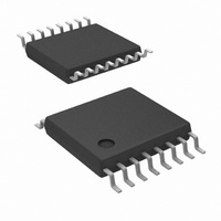
LM5026MT/NOPB National Semiconductor, LM5026MT/NOPB Datasheet - Page 15

LM5026MT/NOPB
Manufacturer Part Number
LM5026MT/NOPB
Description
CURRENT MODE-ACTIVE RESET
Manufacturer
National Semiconductor
Series
PowerWise®r
Datasheet
1.LM5026MTNOPB.pdf
(22 pages)
Specifications of LM5026MT/NOPB
Pwm Type
Current Mode
Number Of Outputs
2
Frequency - Max
1MHz
Duty Cycle
92.5%
Voltage - Supply
13 V ~ 100 V
Buck
Yes
Boost
Yes
Flyback
Yes
Inverting
Yes
Doubler
No
Divider
No
Cuk
No
Isolated
Yes
Operating Temperature
-40°C ~ 125°C
Package / Case
16-TSSOP
Frequency-max
1MHz
For Use With
LM5026EVAL - BOARD EVALUATION LM5026
Lead Free Status / RoHS Status
Lead free / RoHS Compliant
Other names
*LM5026MT
*LM5026MT/NOPB
LM5026MT
*LM5026MT/NOPB
LM5026MT
Available stocks
Company
Part Number
Manufacturer
Quantity
Price
Company:
Part Number:
LM5026MT/NOPB
Manufacturer:
TI
Quantity:
3 000
Thermal Protection
Internal Thermal Shutdown circuitry is provided to protect the
integrated circuit in the event the maximum junction temper-
ature is exceeded. When activated, typically at 165°C, the
controller is forced into a low power standby state with the
output drivers and the bias regulator disabled. The device will
restart after the thermal hysteresis (typically 25°C). During
thermal shutdown, the soft-start capacitor is fully discharged
and the controller follows a normal start-up sequence after the
junction temperature falls to the operating level.
Applications Information
LINE INPUT (VIN)
The LM5026 contains an internal high voltage start-up regu-
lator that allows the input pin (VIN) to be connected directly
to a nominal 48V line voltage. The voltage applied to the VIN
pin can vary in the range of 13 to 100V with transient capability
to 105V. When power is applied and the UVLO pin potential
is greater than 0.4V, the VCC regulator is enabled and
sources current into an external capacitor connected to the
VCC pin. When the voltage on the VCC pin reaches the reg-
ulation point of 7.7V, the internal voltage reference (REF) is
enabled. The reference regulation set point is 5V. The con-
troller outputs are enabled when the UVLO pin potential is
greater than 1.25V. In typical applications, an auxiliary trans-
former winding is connected through a diode to the VCC pin.
This winding must raise the VCC voltage above 8V to shut off
the internal start-up regulator. It is recommended a filtering
circuit shown in
which may occur at the input supply, in particular when VIN
is operated close to the maximum operating rating.
FIGURE 10. Oscillator Sync I/O Block Diagram
Figure 11
be used to suppress transients,
20147921
15
FOR APPLICATION > 100V
For applications where the system input voltage exceed 100V
or IC power dissipation is a concern, the LM5026 can be
powered from an external start-up regulator as shown in
ure
be connected together, which allows the LM5026 to be oper-
ated below 13V. The voltage at the VCC pin must be greater
than 8V yet not exceed 15V. An auxiliary winding can be used
to reduce the dissipation in the external regulator once the
power converter is active.
UNDER-VOLTAGE LOCKOUT (UVLO)
When the UVLO pin voltage is below 0.4V the controller is in
a low current shutdown mode. When the UVLO pin voltage is
greater than 0.4V but less than 1.25V the controller is in
standby mode. When the UVLO pin voltage is greater than
1.25V the controller is fully enabled. Typically, two external
resistors program the minimum operational voltage for the
power converter as shown in
age is above the 1.25V threshold, an internal 20 μA current
source is enabled to raise the voltage at the UVLO pin, thus
providing threshold hysteresis. Resistance values for R1 and
R2 can be determined from:
Where V
desired UVLO hysteresis at V
is to be enabled when V
V
calculates to 5.9 kΩ. The voltage at the UVLO pin should not
exceed 6V at any time. Be sure to check both the power and
voltage rating for the selected R1 resistor.
Remote configuration of the controller’s operational modes
can be accomplished with open drain device(s) connected to
the UVLO pin as shown in
PWR
12. In this configuration, the VIN and the VCC pins should
FIGURE 12. Start-Up Regulator for V
is decreased to 30V, R1 calculates to 150 kΩ, and R2
PWR
FIGURE 11. Input Transient Protection
is the desired turn-on voltage and V
R1 = V
PWR
Figure
reaches 33V, and disabled when
HYS
Figure
PWR
/ 20 µA
. For example, if the LM5026
14.
13. When UVLO pin volt-
PWR
20147922
www.national.com
>100V
HYS
20147923
is the
Fig-


