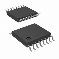
LM5026MT/NOPB National Semiconductor, LM5026MT/NOPB Datasheet - Page 19

LM5026MT/NOPB
Manufacturer Part Number
LM5026MT/NOPB
Description
CURRENT MODE-ACTIVE RESET
Manufacturer
National Semiconductor
Series
PowerWise®r
Datasheet
1.LM5026MTNOPB.pdf
(22 pages)
Specifications of LM5026MT/NOPB
Pwm Type
Current Mode
Number Of Outputs
2
Frequency - Max
1MHz
Duty Cycle
92.5%
Voltage - Supply
13 V ~ 100 V
Buck
Yes
Boost
Yes
Flyback
Yes
Inverting
Yes
Doubler
No
Divider
No
Cuk
No
Isolated
Yes
Operating Temperature
-40°C ~ 125°C
Package / Case
16-TSSOP
Frequency-max
1MHz
For Use With
LM5026EVAL - BOARD EVALUATION LM5026
Lead Free Status / RoHS Status
Lead free / RoHS Compliant
Other names
*LM5026MT
*LM5026MT/NOPB
LM5026MT
*LM5026MT/NOPB
LM5026MT
Available stocks
Company
Part Number
Manufacturer
Quantity
Price
Company:
Part Number:
LM5026MT/NOPB
Manufacturer:
TI
Quantity:
3 000
Layout considerations are critical for the current sense filter.
If a current sense transformer is used, both leads of the trans-
former secondary should be routed to the sense filter com-
ponents and to the IC pins. The ground side of each
transformer should be connected via a dedicated PC board
track to the AGND pin, rather than through the ground plane.
If the current sense circuit employs a sense resistor in the
drive transistor source, low inductance resistor should be
used. In this case, all the noise sensitive low current ground
tracks should be connected in common near the IC, and then
a single connection made to the power ground (sense resistor
ground point). The gate drive outputs of the LM5026 should
have short direct paths to the power MOSFETs in order to
minimize inductance in the PC board traces.
The two ground pins (AGND, PGND) must be connected to-
gether with a short direct connection to avoid jitter due to
relative ground bounce.
If the internal dissipation of the LM5026 produces high junc-
tion temperatures during normal operation, the use of multiple
vias under the IC to a ground place can help conduct heat
away from the IC. Judicious positioning of the PC board within
the end product, along with use of any available air flow
19
(forced or natural convection) can help reduce the junction
temperatures.
Application Circuit Example
The following schematic shows an example of an LM5026
controlled 100W active clamp forward power converter. The
input voltage range (V
age is 3.3V. The output current capability is 30 Amps. Current
sense transformer T2 provides information to the CS pin for
current mode control and current limit protection. The error
amplifiers and reference U3 and U4 provide voltage feedback
via optocoupler U2. Synchronous rectifiers Q3-Q6 minimize
rectification losses in the secondary. An auxiliary winding on
inductor L2 provides power to the LM5026 VCC pin when the
output is in regulation. The input voltage UVLO levels are
≈
The circuit can be shut down by forcing the ON/OFF input (J2)
below 1.25V. An external synchronizing frequency can be ap-
plied to the SYNC input (J11) or like converters can be self-
synchronized by connections of (J3). The regulator output is
current limited at
34V for increasing V
≈
32A.
PWR
PWR
) is 36V to 78V, and the output volt-
, and
≈
32V for decreasing V
www.national.com
PWR
.


