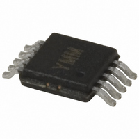
MIC2164-3YMM Micrel Inc, MIC2164-3YMM Datasheet - Page 15

MIC2164-3YMM
Manufacturer Part Number
MIC2164-3YMM
Description
IC PWM BUCK CNTLLR 10MSOP
Manufacturer
Micrel Inc
Series
Hyper Speed Control™r
Type
Step-Down (Buck)r
Datasheet
1.MIC2164YMM.pdf
(39 pages)
Specifications of MIC2164-3YMM
Internal Switch(s)
No
Synchronous Rectifier
Yes
Number Of Outputs
1
Voltage - Output
0.8 ~ 5.5 V
Frequency - Switching
1MHz
Voltage - Input
3 ~ 5.5 V
Operating Temperature
-40°C ~ 125°C
Mounting Type
Surface Mount
Package / Case
10-MSOP, Micro10™, 10-uMAX, 10-uSOP
Voltage - Supply
3 V ~ 28 V
Frequency-max
1.25MHz
Duty Cycle
66%
Pwm Type
Controller
Buck
Yes
Boost
No
Flyback
No
Inverting
No
Doubler
No
Divider
No
Cuk
No
Isolated
No
Lead Free Status / RoHS Status
Lead free / RoHS Compliant
Other names
576-3544-5
Micrel, Inc.
Using the typical V
value is roughly estimated as:
For designs where the current ripple is significant
compared to the load current I
operation, calculating the current limit I
into account that one is sensing the peak inductor
current and that there is a blanking delay of
approximately 150ns.
where
V
T
ΔI
D = Duty Cycle
f
The MOSFET R
temperature; therefore, it is recommended to add a 50%
margin to I
limiting due to increased MOSFET junction temperature
rise. It is also recommended to connect LX pin directly to
the drain of the low-side MOSFET to accurately sense
the MOSFETs R
SW
September 2010
DLY
OUT
L(pp)
= Switching frequency
= Current limit blanking time, 150ns typical
= The output voltage
Figure 4. MIC2164/-2/-3 Current Limiting Circuit
= Inductor current ripple peak-to-peak value
I
CL
CL
=
in the above equation to avoid false current
ΔI
R
130mV
L(pp)
DS(ON)
DS(ON)
DS(ON)
CL
=
I
CL
.
value of 130mV, the current limit
V
+
OUT
≈
V
f
R
OUT
SW
130mV
⋅
DS(ON)
varies 30 to 40% with
(1
⋅
L
L
OUT
−
*
D)
T
DLY
, or for low duty cycle
−
ΔI
CL
L(pp)
2
should take
(2)
(3)
15
MOSFET Gate Drive
The MIC2164/-2/-3 high-side drive circuit is designed to
switch an N-Channel MOSFET. The block diagram of
Figure 1 shows a bootstrap circuit, consisting of D1 (a
Schottky diode is recommended) and C
supplies energy to the high-side drive circuit. Capacitor
C
the voltage on the LX pin is approximately 0V. When the
high-side MOSFET driver is turned on, energy from C
is used to turn the MOSFET on. As the high-side
MOSFET turns on, the voltage on the LX pin increases
to approximately V
C
MOSFET on. The bias current of the high-side driver is
less than 10mA so a 0.1μF to 1μF is sufficient to hold
the gate voltage with minimal droop for the power stroke
(high-side switching) cycle, i.e. ΔBST = 10mA x
3.33μs/0.1μF = 333mV for MIC2164. When the low-side
MOSFET is turned back on, C
D1. A small resistor R
slow down the turn-on time of the high-side N-channel
MOSFET.
The drive voltage is derived from the supply voltage V
The nominal low-side gate drive voltage is V
nominal high-side gate drive voltage is approximately V
– V
approximate 30ns delay between the high-side and low-
side driver transitions is used to prevent current from
simultaneously
MOSFETs.
BST
BST
DIODE
is charged while the low-side MOSFET is on and
floats high while continuing to keep the high-side
, where V
DIODE
flowing
HSD
. Diode D1 is reversed biased and
G
is the voltage drop across D1. An
, which is in series with C
unimpeded
BST
is recharged through
MIC2164/-2/-3/C
M9999-091310-D
BST
through
. This circuit
IN
BST
and the
, can
both
BST
IN
IN
.


