TL494ING ON Semiconductor, TL494ING Datasheet
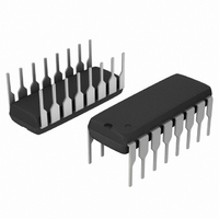
IC PWM VM 16DIP

TL494ING

Manufacturer Part Number
TL494ING
Description
IC PWM VM 16DIP
Manufacturer
ON Semiconductor
Series
SWITCHMODE™r
Datasheet

Specifications of TL494ING

Pwm Type
Voltage Mode
Number Of Outputs
1
Frequency - Max
200kHz
Duty Cycle
50%
Voltage - Supply
7 V ~ 40 V
Buck
No
Boost
No
Flyback
No
Inverting
No
Doubler
No
Divider
No
Cuk
No
Isolated
No
Operating Temperature
-40°C ~ 85°C
Package / Case
16-DIP (0.300", 7.62mm)
Frequency-max
200kHz
Topology
Push-Pull
Output Current
500 mA
Switching Frequency
200 KHz
Duty Cycle (max)
48 %
Operating Supply Voltage
15 V
Maximum Operating Temperature
+ 85 C
Minimum Operating Temperature
- 40 C
Fall Time
40 ns
Mounting Style
Through Hole
Rise Time
100 ns
Synchronous Pin
No
Lead Free Status / RoHS Status
Lead free / RoHS Compliant
Other names
TL494INGOS

Available stocks

Company
Part Number
Manufacturer
Quantity
Price
Part Number:
TL494ING
Manufacturer:
ON Semiconductor
Quantity:
355
TL494, NCV494
SWITCHMODE™ Pulse Width
Modulation Control Circuit
circuit designed primarily for SWITCHMODE power supply control.
Features
Maximum ratings are those values beyond which device damage can occur.
Maximum ratings applied to the device are individual stress limit values (not
normal operating conditions) and are not valid simultaneously. If these limits are
exceeded, device functional operation is not implied, damage may occur and
reliability may be affected.
1. Maximum thermal limits must be observed.
*For additional information on our Pb−Free strategy and soldering details, please
© Semiconductor Components Industries, LLC, 2005
June, 2005 − Rev. 6
MAXIMUM RATINGS
unless otherwise noted.)
download the ON Semiconductor Soldering and Mounting Techniques
Reference Manual, SOLDERRM/D.
Power Supply Voltage
Collector Output Voltage
Collector Output Current
Amplifier Input Voltage Range
Power Dissipation @ T
Thermal Resistance, Junction−to−Ambient
Operating Junction Temperature
Storage Temperature Range
Operating Ambient Temperature Range
Derating Ambient Temperature
The TL494 is a fixed frequency, pulse width modulation control
and Control Changes
Complete Pulse Width Modulation Control Circuitry
On−Chip Oscillator with Master or Slave Operation
On−Chip Error Amplifiers
On−Chip 5.0 V Reference
Adjustable Deadtime Control
Uncommitted Output Transistors Rated to 500 mA Source or Sink
Output Control for Push−Pull or Single−Ended Operation
Undervoltage Lockout
NCV Prefix for Automotive and Other Applications Requiring Site
Pb−Free Packages are Available*
(Each transistor) (Note 1)
TL494B
TL494C
TL494I
NCV494B
Rating
A
(Full operating ambient temperature range applies,
≤ 45°C
Symbol
I
C1
R
V
V
V
V
T
P
T
T
T
C1
qJA
CC
, I
stg
C2
IR
D
A
A
J
C2
,
−55 to +125
−40 to +125
−40 to +125
−0.3 to +42
−40 to +85
0 to +70
Value
1000
500
125
42
42
80
45
1
°C/W
Unit
mW
mA
°C
°C
°C
°C
V
V
V
See detailed ordering and shipping information in the package
dimensions section on page 4 of this data sheet.
Compen/PWN
Comp Input
*This marking diagram also applies to NCV494.
Deadtime
Control
Ground
Noninv
Input
Input
ORDERING INFORMATION
Inv
C
R
C1
T
T
x
A
WL
YY, Y
WW, W
G
1
2
3
4
5
6
7
8
http://onsemi.com
PIN CONNECTIONS
≈ 0.1 V
CASE 751B
+
Error
Amp
CASE 648
D SUFFIX
N SUFFIX
SOIC−16
PDIP−16
Oscillator
1
(Top View)
= B, C or I
= Assembly Location
= Wafer Lot
= Year
= Work Week
= Pb−Free Package
Q1
Publication Order Number:
V
CC
2 Error
5.0 V
Amp
REF
16
*
1
16
+
1
Q2
DIAGRAMS
MARKING
AWLYYWWG
TL494xDG
AWLYWW
16
15
14
13
12
10
11
9
TL494xN
Noninv
Input
Inv
Input
V
Output
Contro
l
V
C2
E2
E1
ref
CC
TL494/D

Related parts for TL494ING

TL494ING Summary of contents

Page 1

... Maximum thermal limits must be observed. *For additional information on our Pb−Free strategy and soldering details, please download the ON Semiconductor Soldering and Mounting Techniques Reference Manual, SOLDERRM/D. © Semiconductor Components Industries, LLC, 2005 June, 2005 − Rev. 6 ...

Page 2

RECOMMENDED OPERATING CONDITIONS Characteristics Power Supply Voltage Collector Output Voltage Collector Output Current (Each transistor) Amplified Input Voltage Current Into Feedback Terminal Reference Output Current Timing Resistor Timing Capacitor Oscillator Frequency ELECTRICAL CHARACTERISTICS For typical values T = 25°C, for ...

Page 3

ELECTRICAL CHARACTERISTICS (V For typical values T = 25°C, for min/max values T A Characteristics ERROR AMPLIFIER SECTION Input Offset Voltage ( (Pin 3) Input Offset Current ( (Pin 3) Input Bias ...

Page 4

... TL494CD TL494CDG TL494CDR2 TL494CDR2G TL494CN TL494CNG TL494IN TL494ING NCV494BDR2* NCV494BDR2G* †For information on tape and reel specifications, including part orientation and tape sizes, please refer to our Tape and Reel Packaging Specifications Brochure, BRD8011/D. *NCV494 −40° +125°C. Guaranteed by design. NCV prefix is for automotive and other applications requiring site and change ...

Page 5

Oscillator 0.12V 4 0.7V Deadtime Control 0.7mA + 1 − Error Amp Feedback PWM 1 Comparator Input Capacitor C T Feedback/PWM Comp. Deadtime Control Flip−Flop Clock Input Flip−Flop Q Flip−Flop Q Output ...

Page 6

Description The TL494 is a fixed−frequency pulse width modulation control circuit, incorporating the primary building blocks required for the control of a switching power supply. (See Figure 1.) An internal−linear sawtooth oscillator is frequency− programmable by two external components, R ...

Page 7

A VOL 1.0 10 100 1 FREQUENCY (Hz) Figure 4. Open Loop Voltage Gain and Phase versus Frequency ...

Page 8

Error Amplifier Under Test + V in − − ref Other Error Amplifier Figure 10. Error−Amplifier Characteristics 15V Each C L Output Q 15pF Transistor E 90% 90 10% 10% t ...

Page 9

Output Voltage of System Error Amp V − ref 2 Positive Output Voltage ref Figure 14. Error−Amplifier Sensing Techniques Output Control V ref Output ...

Page 10

V ref ref Figure 18. Slaving Two or More Control Circuits +V = 8.0V to 20V − 1M 33k ...

Page 11

TL494 50V C R D.T. O.C. Gnd 0.001 47k Figure 21. Pulse Width Modulated Step−Down Converter Test Line Regulation Load Regulation ...

Page 12

G K −T− SEATING PLANE 0.25 (0.010 TL494, NCV494 PACKAGE DIMENSIONS SOIC−16 D SUFFIX CASE 751B−05 ISSUE J −B− 0.25 (0.010 ...

Page 13

−T− 0.25 (0.010 TL494, NCV494 PACKAGE DIMENSIONS PDIP−16 N SUFFIX CASE 648−08 ISSUE T NOTES: 1. DIMENSIONING AND TOLERANCING PER 2. CONTROLLING DIMENSION: ...

Page 14

... Fax: 480−829−7709 or 800−344−3867 Toll Free USA/Canada Email: orderlit@onsemi.com TL494, NCV494 N. American Technical Support: 800−282−9855 Toll Free USA/Canada Japan: ON Semiconductor, Japan Customer Focus Center 2−9−1 Kamimeguro, Meguro−ku, Tokyo, Japan 153−0051 Phone: 81−3−5773−3850 http://onsemi.com 14 ON Semiconductor Website: http://onsemi ...

Related keywords