TL494ING ON Semiconductor, TL494ING Datasheet - Page 3
TL494ING
Manufacturer Part Number
TL494ING
Description
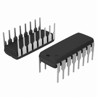
IC PWM VM 16DIP
Manufacturer
ON Semiconductor
Series
SWITCHMODE™r
Datasheet
1.TL494CDR2G.pdf
(14 pages)
Specifications of TL494ING
Pwm Type
Voltage Mode
Number Of Outputs
1
Frequency - Max
200kHz
Duty Cycle
50%
Voltage - Supply
7 V ~ 40 V
Buck
No
Boost
No
Flyback
No
Inverting
No
Doubler
No
Divider
No
Cuk
No
Isolated
No
Operating Temperature
-40°C ~ 85°C
Package / Case
16-DIP (0.300", 7.62mm)
Frequency-max
200kHz
Topology
Push-Pull
Output Current
500 mA
Switching Frequency
200 KHz
Duty Cycle (max)
48 %
Operating Supply Voltage
15 V
Maximum Operating Temperature
+ 85 C
Minimum Operating Temperature
- 40 C
Fall Time
40 ns
Mounting Style
Through Hole
Rise Time
100 ns
Synchronous Pin
No
Lead Free Status / RoHS Status
Lead free / RoHS Compliant
Other names
TL494INGOS
Available stocks
Company
Part Number
Manufacturer
Quantity
Price
Company:

Part Number:
TL494ING
Manufacturer:
ON Semiconductor
Quantity:
355


ELECTRICAL CHARACTERISTICS
For typical values T
ERROR AMPLIFIER SECTION
PWM COMPARATOR SECTION (Test Circuit Figure 11)
DEADTIME CONTROL SECTION (Test Circuit Figure 11)
OSCILLATOR SECTION
UNDERVOLTAGE LOCKOUT SECTION
TOTAL DEVICE
* Standard deviation is a measure of the statistical distribution about the mean as derived from the formula, s
Input Offset Voltage (V
Input Offset Current (V
Input Bias Current (V
Input Common Mode Voltage Range (V
Open Loop Voltage Gain (DV
Unity−Gain Crossover Frequency (V
Phase Margin at Unity−Gain (V
Common Mode Rejection Ratio (V
Power Supply Rejection Ratio (DV
Output Sink Current (V
Output Source Current (V
Input Threshold Voltage (Zero Duty Cycle)
Input Sink Current (V
Input Bias Current (Pin 4) (V
Maximum Duty Cycle, Each Output, Push−Pull Mode
Input Threshold Voltage (Pin 4)
Frequency (C
Standard Deviation of Frequency* (C
Frequency Change with Voltage (V
Frequency Change with Temperature (DT
Turn−On Threshold (V
Standby Supply Current (Pin 6 at V
Average Supply Current
(V
(V
(Zero Duty Cycle)
(Maximum Duty Cycle)
(C
(V
(V
(C
(V
Pin 4
Pin 4
CC
CC
T
CC
T
= 0.01 mF, R
= 0.01 mF, R
= 15 V)
= 40 V)
= 15 V) (See Figure 12)
= 0 V, C
= 0 V, C
T
= 0.001 mF, R
T
T
A
T
T
= 0.01 mF, R
= 0.001 mF, R
= 25°C, for min/max values T
= 12 kW)
= 12 kW, V
O (Pin 3)
(Pin 3)
CC
O (Pin 3)
O (Pin 3)
O (Pin 3)
O (Pin 3)
increasing, I
= 0.7 V)
Pin 4
T
= 2.5 V)
O
Characteristics
= 30 kW)
= 2.5 V)
= 2.5 V)
= 0.7 V)
O
(Pin 4)
= 3.0 V, V
T
T
= 12 kW)
= 0.5 V to 3.5 V, R
= 0 V to 5.25 V)
= 3.5 V)
CC
CC
= 30 kW)
CC
ref
O
T
= 2.0 V)
, All other inputs and outputs open)
= 40 V)
= 33 V, V
ref
= 7.0 V to 40 V, T
= 0.5 V to 3.5 V, R
= 0.001 mF, R
CC
(V
= 1.0 mA)
O
A
CC
= 40 V, T
= 0.5 V to 3.5 V, R
= T
= 15 V, C
low
O
A
= 2.5 V, R
to T
is the operating ambient temperature range that applies, unless otherwise noted.
A
L
T
= 2.0 kW)
= 25°C)
= 30 kW)
high
T
A
TL494, NCV494
http://onsemi.com
= 0.01 mF, R
L
= 25°C)
)
= 2.0 kW)
L
= 2.0 kW)
L
= 2.0 kW)
3
T
= 12 kW, unless otherwise noted.)
Df
Df
Symbol
CMRR
DC
PSRR
I
osc
osc
IB (DT)
A
V
sf
V
V
I
f
I
f
f
I
V
V
I
I
VOL
osc
O−
O
I
CC
ICR
C−
IO
IB
TH
I−
osc
IO
m
max
th
th
+
(DV)
(DT)
Min
0.3
2.0
0.3
5.5
70
65
45
−
−
−
−
−
−
−
−
−
−
0
−
−
−
−
−
−
−
−0.3 to V
−0.1
−4.0
−2.0
6.43
Typ
350
100
2.0
5.0
0.7
2.5
0.7
2.8
3.0
0.1
5.5
7.0
7.0
95
65
90
48
45
40
−
−
CC
−2.0
N
S (X
n = 1
N − 1
n
Max
−1.0
250
−10
4.5
3.3
7.0
10
50
50
12
10
15
− X)
−
−
−
−
−
−
−
−
−
−
−
−
−
2
Unit
deg.
kHz
kHz
mV
mA
mA
mA
mA
mA
nA
dB
dB
dB
mA
mA
%
%
%
%
V
V
V
V
Related parts for TL494ING
Image
Part Number
Description
Manufacturer
Datasheet
Request
R

Part Number:
Description:
ON Semiconductor [VOLTAGE REGULATOR]
Manufacturer:
ON Semiconductor
Datasheet:
Part Number:
Description:
357-036-542-201 CARDEDGE 36POS DL .156 BLK LOPRO
Manufacturer:
ON Semiconductor
Datasheet:
Part Number:
Description:
357-036-542-201 CARDEDGE 36POS DL .156 BLK LOPRO
Manufacturer:
ON Semiconductor
Datasheet:
Part Number:
Description:
357-036-542-201 CARDEDGE 36POS DL .156 BLK LOPRO
Manufacturer:
ON Semiconductor
Datasheet:
Part Number:
Description:
357-036-542-201 CARDEDGE 36POS DL .156 BLK LOPRO
Manufacturer:
ON Semiconductor
Datasheet:
Part Number:
Description:
357-036-542-201 CARDEDGE 36POS DL .156 BLK LOPRO
Manufacturer:
ON Semiconductor
Datasheet:
Part Number:
Description:
357-036-542-201 CARDEDGE 36POS DL .156 BLK LOPRO
Manufacturer:
ON Semiconductor
Datasheet:
Part Number:
Description:
357-036-542-201 CARDEDGE 36POS DL .156 BLK LOPRO
Manufacturer:
ON Semiconductor
Datasheet:
Part Number:
Description:
357-036-542-201 CARDEDGE 36POS DL .156 BLK LOPRO
Manufacturer:
ON Semiconductor
Datasheet:
Part Number:
Description:
357-036-542-201 CARDEDGE 36POS DL .156 BLK LOPRO
Manufacturer:
ON Semiconductor
Datasheet:
Part Number:
Description:
357-036-542-201 CARDEDGE 36POS DL .156 BLK LOPRO
Manufacturer:
ON Semiconductor
Datasheet:
Part Number:
Description:
Manufacturer:
ON Semiconductor
Datasheet:
Part Number:
Description:
Manufacturer:
ON Semiconductor
Datasheet:
Part Number:
Description:
Manufacturer:
ON Semiconductor
Datasheet: