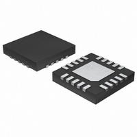
MAX1980ETP+ Maxim Integrated Products, MAX1980ETP+ Datasheet - Page 17

MAX1980ETP+
Manufacturer Part Number
MAX1980ETP+
Description
IC CNTRLR QUICK-PWM 20-TQFN
Manufacturer
Maxim Integrated Products
Datasheet
1.MAX1980ETPT.pdf
(33 pages)
Specifications of MAX1980ETP+
Pwm Type
Controller
Number Of Outputs
1
Frequency - Max
550kHz
Duty Cycle
50%
Voltage - Supply
4 V ~ 28 V
Buck
Yes
Boost
No
Flyback
No
Inverting
No
Doubler
No
Divider
No
Cuk
No
Isolated
No
Operating Temperature
0°C ~ 85°C
Package / Case
20-TQFN Exposed Pad
Frequency-max
550kHz
Input Voltage
4 V to 28 V
Mounting Style
SMD/SMT
Maximum Operating Temperature
+ 100 C
Minimum Operating Temperature
- 40 C
Lead Free Status / RoHS Status
Lead free / RoHS Compliant
Figure 3. “Valley” Current-Limit Threshold Point
guarantee full-load operation under worst-case condi-
tions. Furthermore, the inaccurate current limit mandates
the use of MOSFETs and inductors with excessively high
current and power dissipation ratings.
The slave includes a precision current-limit comparator
that supplements the master’s current-limit circuitry.
The MAX1980 uses CM+ and CM- to differentially
sense the master’s inductor current across a current-
sense resistor, providing a more accurate current limit.
When the master’s current-sense voltage exceeds the
current limit set by ILIM in the slave (see the Dual-Mode
ILIM Input section), the open-drain current-limit com-
parator pulls LIMIT low (Figure 2). Once the master trig-
gers the current limit, a pulse-width-modulated output
signal appears at LIMIT. This signal is filtered and used
to adjust the master’s current-limit threshold.
The gate drive voltage for the high-side, N-channel
MOSFET is generated by the flying capacitor boost cir-
cuit (Figure 4). The capacitor between BST and LX is
alternately charged from the external 5V bias supply
(V
FET’s gate-source terminals.
On startup, the synchronous rectifier (low-side MOS-
FET) forces LX to ground and charges the boost
capacitor to 5V. On the second half of each cycle, the
switch-mode power supply turns on the high-side MOS-
FET by closing an internal switch between BST and DH.
This provides the necessary gate-to-source voltage to
turn on the high-side switch, an action that boosts the
5V gate drive signal above the system’s main supply
voltage (V+).
DD
Driver Disable for Multiphase DC-DC Converter
) and placed in parallel with the high-side MOS-
0
High-Side Gate Driver Supply (BST)
______________________________________________________________________________________
I
LIMIT(VALLEY)
TIME
= I
LOAD(MAX)
Quick-PWM Slave Controller with
( )
2 - LIR
2η
I
I
I
PEAK
LOAD
LIMIT
The DH and DL drivers are optimized for driving moder-
ately sized, high-side and larger, low-side power
MOSFETs. This is consistent with the low duty factor
seen in the notebook CPU environment, where a large
V
cuit monitors the DL output and prevents the high-side
FET from turning on until DL is fully off. There must be a
low-resistance, low-inductance path from the DL driver
to the MOSFET gate in order for the adaptive dead-time
circuit to work properly. Otherwise, the sense circuitry in
the MAX1980 will interpret the MOSFET gate as “off”
while there is actually charge still left on the gate. Use
very short, wide traces (50mils to 100mils wide if the
MOSFET is 1 inch from the device). The dead time at
the other edge (DH turning off) is determined by a fixed
35ns internal delay.
The internal pulldown transistor that drives DL low is
robust, with a 0.4Ω (typ) on-resistance. This helps pre-
vent DL from being pulled up during the fast rise-time
of the LX node, due to capacitive coupling from the
drain to the gate of the low-side synchronous-rectifier
MOSFET. However, for high-current applications, some
combinations of high- and low-side FETs may cause
excessive gate-drain coupling, leading to poor efficien-
cy, EMI, and shoot-through currents. This is often reme-
died by adding a resistor less than 5Ω in series with
BST, which increases the turn-on time of the high-side
FET without degrading the turn-off time (Figure 4).
Figure 4. High-Side Gate Driver Boost Circuitry
IN
- V
OUT
MAX1980
differential exists. An adaptive dead-time cir-
BST
DH
V+
LX
MOSFET Gate Drivers (DH, DL)
(R
BST
)*
( )*OPTIONAL—THE RESISTOR REDUCES
THE SWITCHING-NODE RISE TIME.
D
C
BST
C
BYP
BST
INPUT
(V
IN
N
)
H
L
17


