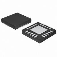
MAX1980ETP+ Maxim Integrated Products, MAX1980ETP+ Datasheet - Page 24

MAX1980ETP+
Manufacturer Part Number
MAX1980ETP+
Description
IC CNTRLR QUICK-PWM 20-TQFN
Manufacturer
Maxim Integrated Products
Datasheet
1.MAX1980ETPT.pdf
(33 pages)
Specifications of MAX1980ETP+
Pwm Type
Controller
Number Of Outputs
1
Frequency - Max
550kHz
Duty Cycle
50%
Voltage - Supply
4 V ~ 28 V
Buck
Yes
Boost
No
Flyback
No
Inverting
No
Doubler
No
Divider
No
Cuk
No
Isolated
No
Operating Temperature
0°C ~ 85°C
Package / Case
20-TQFN Exposed Pad
Frequency-max
550kHz
Input Voltage
4 V to 28 V
Mounting Style
SMD/SMT
Maximum Operating Temperature
+ 100 C
Minimum Operating Temperature
- 40 C
Lead Free Status / RoHS Status
Lead free / RoHS Compliant
If the master/slave converter is operated as the second
stage of a two-stage power-conversion system, tanta-
lum input capacitors are acceptable. In either configu-
ration, choose an input capacitor that exhibits less than
+10°C temperature rise at the RMS input current for
optimal circuit longevity.
Most of the following MOSFET guidelines focus on the
challenge of obtaining high load-current capability
when using high-voltage (>20V) AC adapters. Low-cur-
rent applications usually require less attention.
The high-side MOSFET (N
the resistive losses plus the switching losses at both
V
Ideally, the losses at V
to losses at V
the losses at V
losses at V
Conversely, if the losses at V
higher than the losses at V
the size of N
the minimum power dissipation occurs where the resis-
tive losses equal the switching losses.
Choose a low-side MOSFET that has the lowest possi-
ble on-resistance (R
sized package (i.e., one or two SO-8s, DPAK or
D
DL gate driver can supply sufficient current to support
the gate charge and the current injected into the para-
sitic gate-to-drain capacitor caused by the high-side
MOSFET turning on; otherwise, cross-conduction prob-
lems may occur.
Worst-case conduction losses occur at the duty factor
extremes. For the high-side MOSFET (N
case power dissipation due to resistance occurs at the
minimum input voltage:
Generally, a small high-side MOSFET is desired to
reduce switching losses at high input voltages.
However, the R
power-dissipation often limits how small the MOSFET
can be. Again, the optimum occurs when the switching
losses equal the conduction (R
side switching losses don’t usually become an issue
until the input is greater than approximately 15V.
Quick-PWM Slave Controller with
Driver Disable for Multiphase DC-DC Converter
24
IN(MIN)
2
PAK), and is reasonably priced. Make sure that the
______________________________________________________________________________________
PD N
(
and V
H
IN(MAX)
Re
H
IN(MAX)
. If V
sistive
IN(MAX)
IN(MIN)
DS(ON)
, consider increasing the size of N
IN
MOSFET Power Dissipation
)
, with lower losses in between. If
does not vary over a wide range,
DS(ON)
=
Power MOSFET Selection
. Calculate both of these sums.
IN(MIN)
are significantly higher than the
required to stay within package
V
H
OUT
V
IN
) must be able to dissipate
IN(MIN)
), comes in a moderate-
should be roughly equal
IN(MAX)
DS(ON)
I
LOAD
, consider reducing
η
are significantly
) losses. High-
2
H
R
), the worst-
DS ON
(
)
H
.
Calculating the power dissipation of the high-side
MOSFET (N
must allow for difficult quantifying factors that influence
the turn-on and turn-off times. These factors include the
internal gate resistance, gate charge, threshold volt-
age, source inductance, and PC board layout charac-
teristics. The following switching-loss calculation
provides only a very rough estimate and is no substi-
tute for breadboard evaluation, preferably including
verification using a thermocouple mounted on N
where C
and I
(1A typ).
Switching losses in the high-side MOSFET can become
an insidious heat problem when maximum AC adapter
voltages are applied, due to the squared term in the C
✕
MOSFET chosen for adequate R
voltages becomes extraordinarily hot when biased from
V
lower parasitic capacitance.
For the low-side MOSFET (N
dissipation always occurs at maximum input voltage:
The worst case for MOSFET power dissipation occurs
under heavy overloads that are greater than I
but are not quite high enough to exceed the current limit
and cause the fault latch to trip. To protect against this
possibility, “overdesign” the circuit to tolerate:
where I
allowed by the current-limit circuit, including threshold
tolerance and on-resistance variation. The MOSFETs
must have a good-sized heatsink to handle the over-
load power dissipation.
Choose a Schottky diode (D1) with a forward voltage low
enough to prevent the low-side MOSFET body diode
from turning on during the dead time. As a general rule,
select a diode with a DC current rating equal to 1/(3
the load current. This diode is optional and can be
removed if efficiency is not critical.
IN(MAX)
PD N
V
IN
PD N Switching
(
GATE
2
I
L
✕
LOAD
(
VALLEY(MAX)
RSS
Re
, consider choosing another MOSFET with
ƒ SW
H
sistive
is the peak gate-drive source/sink current
H
) due to switching losses is difficult since it
is the reverse transfer capacitance of N
=
switching-loss equation. If the high-side
η
I
VALLEY MAX
)
=
1
)
=
−
is the maximum valley current
(
(
V
V
IN MAX
IN MAX
V
OUT
(
(
)
L
+
), the worst-case power
)
)
I
LOAD MAX
)
I
DS(ON)
GATE
2
C
I
RSS SW LOAD
LOAD
(
η
η
2
f
at low battery
)
LIR
I
2
LOAD(MAX)
R
DS ON
H
:
(
η
) of
)
H


