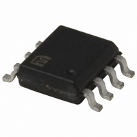
MIC2196BM Micrel Inc, MIC2196BM Datasheet - Page 8

MIC2196BM
Manufacturer Part Number
MIC2196BM
Description
IC PWM BST FLYBCK CM 8SOIC
Manufacturer
Micrel Inc
Datasheet
1.MIC2196YM.pdf
(12 pages)
Specifications of MIC2196BM
Pwm Type
Current Mode
Number Of Outputs
1
Frequency - Max
440kHz
Duty Cycle
85%
Voltage - Supply
2.9 V ~ 14 V
Buck
No
Boost
Yes
Flyback
Yes
Inverting
No
Doubler
No
Divider
No
Cuk
No
Isolated
No
Operating Temperature
-40°C ~ 125°C
Package / Case
8-SOIC (3.9mm Width)
Frequency-max
440kHz
Input Voltage
14V
Frequency
400kHz
Power Dissipation Pd
285mW
Supply Voltage Range
2.9V To 14V
Digital Ic Case Style
SOIC
No. Of Pins
8
Operating Temperature Range
-40°C To +125°C
Lead Free Status / RoHS Status
Contains lead / RoHS non-compliant
Available stocks
Company
Part Number
Manufacturer
Quantity
Price
Company:
Part Number:
MIC2196BM
Manufacturer:
SIEMENS
Quantity:
5 510
Part Number:
MIC2196BM
Manufacturer:
MICREL/麦瑞
Quantity:
20 000
Company:
Part Number:
MIC2196BM TR
Manufacturer:
MICREL
Quantity:
1 486
Company:
Part Number:
MIC2196BMTR
Manufacturer:
MICREL
Quantity:
1 423
A block diagram of the MIC2196 PWM current mode
control loop is shown in Figure 1. The inductor current is
sensed by measuring the voltage across a resistor,
R
this signal. A ramp is added to this signal to provide
slope compensation, which is required in current mode
control to prevent unstable operation at duty cycles
greater than 50%.
A transconductance amplifier is used as an error
amplifier, which compares an attenuated output voltage
with a reference voltage. The output of the error amplifier
is compared to the current sense waveform in the PWM
block. When the current signal rises above the error
voltage, the comparator turns off the low-side drive. The
error signal is brought out to the COMP pin (pin 1) to
provide access to the output of the error amplifier. This
allows the use of external components to stabilize the
voltage loop.
Current Sensing and Overcurrent Protection
The inductor current is sensed during the switch on time
by a current sense resistor located between the source
of the MOSFET and ground (R
Exceeding the current limit threshold will immediately
terminate the gate drive of the N-Channel MOSFET, Q1.
This forces the Q1 to operate at a reduced duty cycle,
which lowers the output voltage. In a boost converter,
the overcurrent limit will not protect the power
supply or load during a severe overcurrent condition
or short circuit condition. If the output is short-
circuited to ground, current will flow from the input,
through the inductor and output diode to ground. Only
the impedance of the source and components limits the
current.
The mode of operation (continuous or discontinuous),
the minimum input voltage, maximum output power and
the minimum value of the current limit threshold
determine the value of the current sense resistor.
Discontinuous mode is where all the energy in the
inductor is delivered to the output at each switching
cycle. Continuous mode of operation occurs when
current always flows in the inductor, during both the low-
side MOSFET on and off times. The equations below will
help to determine the current sense resistor value for
each operating mode.
The critical value of output current in a boost converter is
calculated below. The operating mode is discontinuous if
the output current is below this value and is continuous if
above this value.
where:
Micrel, Inc.
September 2008
SENSE
. The current sense amplifier buffers and amplifies
η is the efficiency of the boost converter
I
CRIT
=
V
IN
2
2
×
×
fs
(
V
×
O
L
−
×
V
V
IN
O
)
2
×
η
SENSE
in Figure 1).
8
Maximum Peak Current in Discontinuous Mode:
The peak inductor current is:
where:
The maximum value of current sense resistor is:
where:
Maximum Peak Current in Continuous Mode:
The peak inductor current is equal to the average
inductor current plus one half of the peak to peak
inductor current.
The peak inductor current is:
where:
V
However, the voltage drop across the inductor winding
resistance and low-side MOSFET on-resistance must be
accounted for at the lower input voltages that the
MIC2196 operates at:
L
may be approximated as V
V
L is the value of the boost inductor
fs is the switching frequency
V
I
V
V
L is the value of the boost inductor
fs is the switching frequency
η is the efficiency of the boost converter
V is the minimum current sense threshold of the
CS pin.
I
V
V
L is the value of the boost inductor
fs is the switching frequency
η is the efficiency of the boost converter
V
I
R
I
I
O
O
IND(pk)
IND(pk)
IND(pk)
IN
O
O
IN
O
IN
L
SENSE
is the maximum output current
is the maximum output current
is the voltage across the inductor
is the output voltage
is the output voltage
is the output voltage
is the minimum input voltage
is the minimum input voltage
is the minimum input voltage
=
=
=
=
I
V
IND(ave)
V
V
2
I
O
IN
IND(pk)
SENSE
×
×
×
I
I
O
η
O
×
+
+
(
L
1
2
V
V
×
O
×
L
2
fs
I
IN
−
IND(pp)
×
×
η
(
for higher input voltage.
V
V
×
O
O
V
×
−
IN
fs
V
)
IN
×
M9999-092908
L
×
η
)
MIC2196


