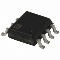
MIC2196BM Micrel Inc, MIC2196BM Datasheet - Page 9

MIC2196BM
Manufacturer Part Number
MIC2196BM
Description
IC PWM BST FLYBCK CM 8SOIC
Manufacturer
Micrel Inc
Datasheet
1.MIC2196YM.pdf
(12 pages)
Specifications of MIC2196BM
Pwm Type
Current Mode
Number Of Outputs
1
Frequency - Max
440kHz
Duty Cycle
85%
Voltage - Supply
2.9 V ~ 14 V
Buck
No
Boost
Yes
Flyback
Yes
Inverting
No
Doubler
No
Divider
No
Cuk
No
Isolated
No
Operating Temperature
-40°C ~ 125°C
Package / Case
8-SOIC (3.9mm Width)
Frequency-max
440kHz
Input Voltage
14V
Frequency
400kHz
Power Dissipation Pd
285mW
Supply Voltage Range
2.9V To 14V
Digital Ic Case Style
SOIC
No. Of Pins
8
Operating Temperature Range
-40°C To +125°C
Lead Free Status / RoHS Status
Contains lead / RoHS non-compliant
Available stocks
Company
Part Number
Manufacturer
Quantity
Price
Company:
Part Number:
MIC2196BM
Manufacturer:
SIEMENS
Quantity:
5 510
Part Number:
MIC2196BM
Manufacturer:
MICREL/麦瑞
Quantity:
20 000
Company:
Part Number:
MIC2196BM TR
Manufacturer:
MICREL
Quantity:
1 486
Company:
Part Number:
MIC2196BMTR
Manufacturer:
MICREL
Quantity:
1 423
where:
The maximum value of current sense resistor is:
where:
The current sense pin, CS, is noise sensitive due to the
low
measurement is referenced to the signal ground pin of
the MIC2196. The current sense resistor ground should
be located close to the IC ground. Make sure there are
no high currents flowing in this trace. The PCB trace
between the high side of the current sense resistor and
the CS pin should also be short and routed close to the
ground connection. The input to the internal current
sense amplifier has a 30ns dead time at the beginning of
each switching cycle. This dead time prevents leading
edge current spikes from prematurely terminating the
switching cycle. A small RC filter between the current
sense pin and current sense resistor may help to
attenuate larger switching spikes or high frequency
switching noise. Adding the filter slows down the current
sense signal, which has the effect of slightly raising the
overcurrent limit threshold.
MOSFET Gate Drive
The MIC2196 converter drives a low-side N-Channel
MOSFET. The driver for the OUTN pin has a 2Ω typical
source and sink impedance. The V
for the gate drive circuit. The maximum supply voltage to
the V
MOSFET Selection
In a boost converter, the V
approximately equal to the output voltage. The maximum
V
for ringing and spikes in addition to the output voltage.
The V
The V
must be low enough to operate at the minimum V
voltage to guarantee the boost converter will start up.
The maximum amount of MOSFET gate charge that can
be driven is limited by the power dissipation in the
MIC2196. The power dissipated by the gate drive
circuitry is calculated below:
Micrel, Inc.
September 2008
DS
rating of the MOSFET must be high enough to allow
IN
IN
signal
GS
pin is 14V.
R
R
switching MOSFET
V
of the CS pin.
R
P_gate_dri
V
pin supplies the N-Channel gate drive voltage.
SENSE
WINDING
DSON
threshold voltage of the N-channel MOSFET
L
SENSE
=
V
level.
IN
is the on resistance of the low side
is the minimum current sense threshold
=
is the winding resistance of the inductor
−
V
I
ve
IND(pk)
V
V
SENSE
O
IN
=
×
The
×
Q_gate
I
O
η
×
(
R
current
WINDING
DS
×
V
IN
IN
of the MOSFET is
pin is the supply pin
×
fs
+
sense
R
DSON
)
voltage
IN
9
where:
The graph in Figure 4 shows the total gate charge which
can be driven by the MIC2196 over the input voltage
range. Higher gate charge will slow down the turn-on
and turn-off times of the MOSFET, which increases
switching losses.
External Schottky Diode
In a boost converter topology, the boost diode, D1 must
be rated to handle the peak and average current. The
average current through the diode is equal to the
average output current of the boost converter. The peak
current is calculated in the current limit section of this
specification.
For the MIC2196, Schottky diodes are recommended
when they can be used. They have a lower forward
voltage drop than ultra-fast rectifier diodes, which lowers
power dissipation and improves efficiency. They also do
not have a recovery time mechanism, which results in
less ringing and noise when the diode turns off. If the
output voltage of the circuit prevents the use of a
Schottky diode, then only ultra-fast recovery diodes
should be used. Slower diodes will dissipate more power
in both the MOSFET and the diode. The will also cause
excessive ringing and noise when the diode turns off.
Reference, Enable and UVLO Circuits
The output drivers are enabled when the following
conditions are satisfied:
The internal bias circuitry generates a 1.245V bandgap
reference for the voltage error amplifier and a 3V V
voltage for the internal supply bus. The V
decoupled to ground with a 1μF ceramic capacitor.
•
•
Figure 4. MIC2196 Frequency vs. Gate Charge
Q_gate is the total gate charge of the external
MOSFET
The V
undervoltage threshold.
The voltage on the enable pin is greater than the
enable UVLO threshold.
DD
250
200
150
100
50
0
0
voltage (pin 5) is greater than its
2
Max. Gate Charge
INPUT VOLTAGE (V)
4
6
8 10 12 14
M9999-092908
DD
pin must be
MIC2196
DD


