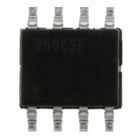
SC2596SETRT Semtech, SC2596SETRT Datasheet - Page 9

SC2596SETRT
Manufacturer Part Number
SC2596SETRT
Description
IC INTEGRTD DDR TERM REG 8-SOIC
Manufacturer
Semtech
Datasheet
1.SC2596SETRT.pdf
(14 pages)
Specifications of SC2596SETRT
Applications
Converter, DDR
Number Of Outputs
1
Operating Temperature
-40°C ~ 105°C
Mounting Type
Surface Mount
Package / Case
8-SOIC
Lead Free Status / RoHS Status
Lead free / RoHS Compliant
Voltage - Output
-
Voltage - Input
-
Other names
SC2596SETR
Available stocks
Company
Part Number
Manufacturer
Quantity
Price
Company:
Part Number:
SC2596SETRT
Manufacturer:
SEMTECH
Quantity:
15 000
Part Number:
SC2596SETRT
Manufacturer:
SEMTECH/美国升特
Quantity:
20 000
Thermal shutdown
The SC2596 has built-in thermal detected circuit to pre-
vent this device from over temperature and damage.
The SC2596 goes into shunt down mode when tem-
perature is higher than 165
will release when the temperature of device drop down
by 10
AVCC and PVCC
AVCC and PVCC are the input supply pins for the SC2596.
AVCC is supply voltage for all the internal control circuitry.
The AVCC voltage has to be greater than its UVLO thresh-
old voltage (2.1V typical) to allow the SC2596 to be nor-
mal operation.
The PVCC pin provides the rail voltage from where the
VTT pin draws load current. There is a limitation between
AVCC and PVCC. The PVCC voltage must be less or equal
to AVCC voltage to ensure the correct VTT output voltage
regulation.
VSENSE
VSENSE pin is a feedback pin from VTT plane. VTT plane
is always a narrow and long strip plane in most
montherboard applications. This long strip plane will
© 2009 Semtech Corp.
Overview
Double Data Rate (DDR) SDRAM was defined by JEDEC
1997. Its clock speed is the same as previous SDRAM
but data transfer speed is twice than previous SDRAM.
By now, the requirement voltage range is changed from
3.3V to 2.5V or 1.8V; the power dissipation is smaller
than SDRAM. For above reasons, it is very popular and
widely used in M/B, N/B, Video-cards, CD ROM drives,
Disk drives.
Regarding the DDR power management solution, there
are two topologies can be selected for system design-
ers. One is switching mode regulator that has bigger sink/
source current capability, but the cost is higher and needs
more board space. Another solution is linear mode regu-
lator, which costs less, and needs less board space. For
two DIMM motherboards, system designers usually
choose the linear mode regulator for DDR power man-
agement solution.
POWER MANAGEMENT
Application Information
O
C.
O
C. The protection condition
9
cause a large trace inductance and trace resistance.
Consider the load transient condition, a fast load cur-
rent going through VTT strip plane will create a voltage
spike on VTT plane and a DC voltage drop for load cur-
rent. It is recommanded the VSENSE pin should be con-
nected center of VTT plane to improve regulation and
transient response.
A longer trace of VSENSE may pick up noise and cause
the error of load regulation. Hence designer should avoid
a longer trace between VSENSE to VTT plane. A 100nF
ceramic capacitor close to VSENSE pin is required.
VREF
VREF pin is an output pin to provid internal reference
voltage. System designer can use the voltage for
Northbridge chipset and memory. It is necessary to add
a ceramic capacitor (100nF) from VREF pin to ground
with shortest trace.
Typical Application Circuits & Waveforms
Four different application circuits are shown below in Fig-
ure 1, Figure 2, Figure 3 and Figure 4. Each circuit is
designed for a specific condition.
below for recommended power up sequencing.
Application_1: Standard SSTL-2 Application
The AVCC pin, PVCC pin and the V
together for SSTL-2 application (Figure 1). It only needs
a 2.5V power rail for normal operation. System designer
can save the PCB space and reduce the cost.
VREF/1.25V
VDDQ/EN=2.5V
Figure 1: Standard SSTL-2 application.
0
Csense
Csense
100nF
100nF
100nF
100nF
CREF
CREF
1
2
3
4
GND
EN
VSENSE
VREF
SC2596
SC2596
VDDQ
PVCC
AVCC
VTT
8
7
6
5
DDQ
See Note a. and b.
CIN1
CIN1
pin can be tied
1uF
1uF
www.semtech.com
SC2596
CIN2
CIN2
100uF
100uF
COUT
COUT
220uF
220uF
VTT/1.25V


