ISL62884CHRTZ Intersil, ISL62884CHRTZ Datasheet - Page 15

ISL62884CHRTZ
Manufacturer Part Number
ISL62884CHRTZ
Description
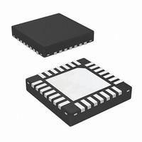
IC REG PWM SGL PHASE 28WQFN
Manufacturer
Intersil
Datasheet
1.ISL62884CHRTZ.pdf
(30 pages)
Specifications of ISL62884CHRTZ
Applications
Controller, Intel IMVP-6
Voltage - Input
4.5 ~ 25 V
Number Of Outputs
1
Voltage - Output
0.0125 ~ 1.5 V
Operating Temperature
-10°C ~ 100°C
Mounting Type
Surface Mount
Package / Case
28-WQFN
Rohs Compliant
Yes
Lead Free Status / RoHS Status
Lead free / RoHS Compliant
Differential Sensing
Figure 9 also shows the differential voltage sensing
scheme. VCC
voltage sensing signals from the processor die. A unity
gain differential amplifier senses the VSS
and adds it to the DAC output. The error amplifier
regulates the inverting and the non-inverting input
voltages to be equal, therefore:
Rewriting Equation 3 and substituting Equation 2 gives:
Equation 4 is the exact equation required for load line
implementation.
The VCC
processor die. The feedback will be open circuit in the
absence of the processor. As shown in Figure 9, it is
recommended to add a “catch” resistor to feed the VR
local output voltage back to the compensator, and add
another “catch” resistor to connect the VR local output
ground to the RTN pin. These resistors, typically
10Ω ~100Ω, will provide voltage feedback if the system is
powered up without a processor installed.
CCM Switching Frequency
The R
sets the VW windows size, which therefore sets the
switching frequency. When the ISL62884C is in
continuous conduction mode (CCM), the switching
frequency is not absolutely constant due to the nature of
the R
Modulator” on page 11, the effective switching frequency
will increase during load insertion and will decrease
during load release to achieve fast response. On the
other hand, the switching frequency is relatively constant
at steady state. Variation is expected when the power
stage condition, such as input voltage, output voltage,
load, etc. changes. The variation is usually less than 15%
and doesn’t have any significant effect on output voltage
ripple magnitude. Equation 5 gives an estimate of the
frequency-setting resistor R
approximately 300kHz switching frequency. Lower
resistance gives higher switching frequency.
Modes of Operation
VCC
DPRSTP# DPRSLPVR OPERATIONAL MODE
VCC
R
FSET
0
0
1
1
SENSE
SENSE
3™
TABLE 2. ISL62884C MODES OF OPERATION
FSET
(
kΩ
SENSE
modulator. As explained in “Multiphase R3™
)
+
resistor between the COMP and the VW pins
–
=
V
VSS
SENSE
(
DROOP
Period μs
and VSS
0
1
0
1
SENSE
and VSS
(
=
V
) 0.29
=
SENSE
DAC
–
V
15
DAC
1-phase CCM
1-phase CCM
1-phase CCM
FSET
1-phase DE
+
SENSE
)
VSS
–
×
signals come from the
2.65
R
value. 8kΩ R
DROOP
SENSE
are the remote
×
SENSE
I
DROOP
SLEW RATE
FSET
(mV/µs)
voltage
2.5
2.5
10
10
ISL62884C
(EQ. 3)
(EQ. 4)
(EQ. 5)
gives
Table 2 shows the ISL62884C operational modes,
programmed by the logic status of the DPRSLPVR pin and
the DPRSTP# pin. The ISL62884C enters 1-phase DE
mode when there is DPRSLPVR = 0 and DPRSLPVR = 1.
DPRSLPVR logic status also controls the output voltage
slew rate.
Dynamic Operation
The ISL62884C responds to VID changes by slewing to
the new voltage at a slew rate programmed by the logic
status on the DPRSLPVR pin, as Table 2 shows. The slew
rate is 10mV/µs for DPRSLPVR = 0 and is 1/4 of that for
DPRSLPVR = 1. As the output approaches the VID
command voltage, the dv/dt moderates to prevent
overshoot.
When the ISL62884C is in DE mode, it will actively drive
the output voltage up when the VID changes to a higher
value. Thus, will resume DE mode operation after
reaching the new voltage level. If the load is light enough
to warrant DCM, it will enter DCM after the inductor
current has crossed zero for four consecutive cycles. The
ISL62884C will remain in DE mode when the VID
changes to a lower value. The output voltage will decay
to the new value and the load will determine the slew
rate.
During load insertion response, the Fast Clock function
increases the PWM pulse response speed. The
ISL62884C monitors the VSEN pin voltage and compares
it to 100ns-filtered version. When the unfiltered version
is 20mV below the filtered version, the controller knows
there is a fast voltage dip due to load insertion, hence
issues an additional master clock signal to deliver a PWM
pulse immediately.
The R
forward. The output voltage is insensitive to a fast slew
rate input voltage change.
Protections
The ISL62884C provides overcurrent, undervoltage,
and overvoltage protections.
The ISL62884C determines overcurrent protection
(OCP) by comparing the average value of the droop
current I
threshold. It declares OCP when I
threshold for 120µs. A resistor R
pin to GND programs the OCP current source threshold,
as well as the overshoot reduction function (to be
discussed in later sections), as Table 3 shows. It is
recommended to use the nominal R
ISL62884C detects the R
start-up, and sets the internal OCP threshold
accordingly. It remembers the R
VR_ON signal drops below the POR threshold.
3
™ modulator intrinsically has voltage feed
DROOP
with an internal current source
comp
value at the beginning of
comp
comp
DROOP
comp
value until the
from the COMP
is above the
value. The
March 16, 2010
FN7591.0


