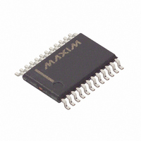
MAX1778EUG+ Maxim Integrated Products, MAX1778EUG+ Datasheet - Page 24

MAX1778EUG+
Manufacturer Part Number
MAX1778EUG+
Description
IC DCDC CONV MULTI OUT 24TSSOP
Manufacturer
Maxim Integrated Products
Datasheet
1.MAX1778EUG.pdf
(39 pages)
Specifications of MAX1778EUG+
Applications
Converter, TFT, LCD
Voltage - Input
2.7 ~ 5.5 V
Number Of Outputs
5
Voltage - Output
2.7 ~ 13 V
Operating Temperature
0°C ~ 85°C
Mounting Type
Surface Mount
Package / Case
24-TSSOP
Lead Free Status / RoHS Status
Lead free / RoHS Compliant
Quad-Output TFT LCD DC-DC
Converters with Buffer
(I
1ms, soft-start enters phase II, and the current limit is
increased by another 25%. This process is repeated for
phase III. The maximum 1.5A (typ) current limit is
reached within 3072 clock cycles or when the output
reaches regulation, whichever occurs first (see the
startup waveforms in the Typical Operating
Characteristics).
For the charge pumps (MAX1778/MAX1880/
MAX1881/MAX1882 only), soft-start is achieved by con-
trolling the rate of rise of the output voltage. Both
charge-pump output voltages are controlled to be in
regulation within 4096 clock cycles, irregardless of out-
put capacitance and load, limited only by the charge
pump’s output impedance. Although the MAX1883/
MAX1884/MAX1885 controllers do not include the
charge pumps, the soft-start logic still contains the
4096 clock cycle startup periods for both charge
pumps.
The MAX1778/MAX1880–MAX1885 feature dual mode
operation to allow operation with either a preset fault
trip level or an adjustable trip level for the step-up con-
verter and positive charge-pump outputs. Connect FLT-
SET to GND to select the preset 0.9
threshold. The fault trip level may also be adjusted by
connecting a voltage divider from REF to FLTSET
(Figure 8). For greatest accuracy, the total load on the
reference (including current through the negative
charge-pump feedback resistors) should not exceed
50µA so that VREF is guaranteed to be in regulation
(see Electrical Characteristics Table). Therefore, select
R10 in the 100kΩ to 1MΩ range, and calculate R9 with
the following equation:
where V
x V
a maximum value of 50nA. For 1% error, the current
through R10 should be at least 100 times the FLTSET
input bias current (I
Once RDY is low, if the output of the main regulator or
either low-power charge pump falls below its fault
detection threshold, or if the input drops below its
undervoltage threshold, then RDY goes high imped-
ance and all outputs shut down; however, the reference
remains active. After removing the fault condition, tog-
gle shutdown (below 0.8V) or cycle the input voltage
(below 0.2V) to clear the fault latch and reactivate the
device.
24
LX(MAX)
REF
______________________________________________________________________________________
to 0.85 x V
REF
). If the output does not reach regulation within
R9 = R10 [(V
= 1.25V, and V
REF
FLTSET
. FLTSET’s input bias current has
Fault Trip Level (FLTSET)
REF
).
FLTSET
/ V
FLTSET
may range from 0.67
Fault Condition
) - 1]
✕
V
REF
fault
The reference fault threshold is 1.05V. For the step-up
converter and positive charge-pump, the fault trip level is
set by FLTSET (see Fault Trip Level). For the negative
charge pump, the fault threshold measured at the
charge-pump’s feedback input (FBN) is 140mV (typ).
Power ready is an open-drain output. When the power-
up sequence for the main step-up converter and low-
power charge pumps has properly completed, the 14V
MOSFET turns on and pulls RDY low with a 125Ω (typ)
on-resistance. If a fault is detected on any of these
three outputs, the internal open-drain MOSFET appears
as a high impedance. Connect a 100kΩ pullup resistor
between RDY and IN for a logic-level output.
The voltage at REF is nominally 1.25V. The reference
can source up to 50µA with good load regulation (see
Typical Operating Characteristics). Connect a 0.22µF
ceramic bypass capacitor between REF and GND.
Thermal-overload protection limits total power dissipa-
tion in the MAX1778/MAX1880–MAX1885. When the
junction temperature exceeds T
sensor activates the fault protection, which shuts down
the controller, allowing the IC to cool. Once the device
cools down by 15°C, toggle shutdown (below 0.8V) or
cycle the input voltage (below 0.2V) to clear the fault
latch and reactivate the controller. Thermal-overload
protection protects the controller in the event of fault
conditions. For continuous operation, do not exceed
the absolute maximum junction-temperature rating of
T
The MAX1778/MAX1880–MAX1885s’ maximum power
dissipation depends on the thermal resistance of the IC
package and circuit board, the temperature difference
between the die junction and ambient air, and the rate
of any airflow. The power dissipated in the device
depends on the operating conditions of each regulator
and the buffer.
The step-up controller dissipates power across the
internal N-channel MOSFET as the controller ramps up
the inductor current. In continuous conduction, the
power dissipated internally can be approximated by:
J
= +150°C.
P
Operating Region and Power Dissipation
STEP UP
−
≈
×
⎡
⎢
⎢
⎣
⎛
⎜
⎝
Thermal-Overload Protection
I
R
MAIN MAIN
DS ON
(
V
Voltage Reference (REF)
IN
V
)
D
Power Ready (RDY)
⎞
⎟
⎠
2
J
= +160°C, a thermal
+
12
1
⎛
⎜
⎝
f
OSC
V D
IN
L
⎞
⎟
⎠
2
⎤
⎥
⎥
⎦


