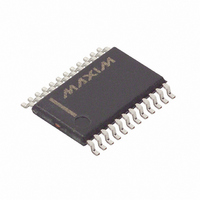
MAX1778EUG+ Maxim Integrated Products, MAX1778EUG+ Datasheet - Page 32

MAX1778EUG+
Manufacturer Part Number
MAX1778EUG+
Description
IC DCDC CONV MULTI OUT 24TSSOP
Manufacturer
Maxim Integrated Products
Datasheet
1.MAX1778EUG.pdf
(39 pages)
Specifications of MAX1778EUG+
Applications
Converter, TFT, LCD
Voltage - Input
2.7 ~ 5.5 V
Number Of Outputs
5
Voltage - Output
2.7 ~ 13 V
Operating Temperature
0°C ~ 85°C
Mounting Type
Surface Mount
Package / Case
24-TSSOP
Lead Free Status / RoHS Status
Lead free / RoHS Compliant
Quad-Output TFT LCD DC-DC
Converters with Buffer
3) Locate all feedback resistive-dividers as close to
4) When using multilayer boards, separate the top sig-
32
Figure 8. 5V Input Monitor Application
regulator and charge-pump power ground plane,
and the inner layer should contain the analog
ground plane and power-ground plane/path for the
V
planes together at one place near the PGND pin.
their respective feedback pins as possible. The
voltage-divider’s center trace should be kept short.
Avoid running any feedback trace near the LX
switching node or the charge-pump drivers. The
resistive-dividers’ ground connections should be to
analog ground (GND).
nal layer and bottom signal layer with a ground
plane between to eliminate capacitive coupling
between fast-charging nodes on the top layer and
______________________________________________________________________________________
COM
V
LDO
= 3.3V
1μF
LDO
V
C6
buffer and LDO. Connect all three ground
IN
INPUT
= 5V
0.01μF
10kΩ
C7
R8
(2) 4.7μF
V
NEGATIVE
NEG
16.4kΩ
C
IN
= -8V
TO LOGIC
R7
Q1
1.0μF
100kΩ
C3
R
RDY
C
LDOOUT
C6
0.01μF
4.7μF
0.22μF
C
REF
0.22μF
316kΩ
R5
C1
49.9kΩ
1.5kΩ
R8
R6
0.1μF
C2
LDOOUT
SUPL
FBL
DRVN
FBN
IN
SHDN
RDY
REF
INTG
PGND
MAX1778
10μH
L1
5) Keep the charge-pump circuitry as close to the IC
6) To maximize output power and efficiency and mini-
Refer to the MAX1778/MAX1880-MAX1885 evaluation
kit for an example of proper board layout.
BUFOUT
FLTSET
SUPN
TGND
SUPB
SUPP
DRVP
BUF-
BUF+
GND
FBP
high-impedance nodes on the bottom layer. The
fast-charging nodes, such as the LX and charge-
pump driver nodes, should not have any other
traces or ground planes near by.
as possible, using wide traces and avoiding vias
when possible. Place 0.1µF ceramic bypass
capacitors near the charge-pump input pins (SUPP
and SUPN) to the PGND pin.
mize output ripple voltage, use extra wide, power
ground traces, and solder the IC’s power ground
pin directly to it.
LX
FB
0.1μF
C4
86.6kΩ
R4
49.9kΩ
10kΩ
R1
R2
R10
100kΩ
C
1.0μF
BUF
750kΩ
R3
R
4.7kΩ
C
COMP
470pF
COMP
30kΩ
R9
BUFFER OUTPUT
V
BUFOUT
= V
SUPB
C5
1.0μF
C
(2) 10μF
REF
OUT
/2
POSITIVE
V
MAIN
V
POS
MAIN
= 20V
= 12V


