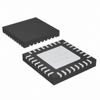
MAX1904ETJ+ Maxim Integrated Products, MAX1904ETJ+ Datasheet - Page 23

MAX1904ETJ+
Manufacturer Part Number
MAX1904ETJ+
Description
IC CNTRLR PWR SPLY LN 32-TQFN
Manufacturer
Maxim Integrated Products
Datasheet
1.MAX1904ETJ.pdf
(33 pages)
Specifications of MAX1904ETJ+
Applications
Controller, Notebook Computers
Voltage - Input
4.2 ~ 30 V
Number Of Outputs
4
Voltage - Output
2.5 ~ 5 V
Operating Temperature
0°C ~ 85°C
Mounting Type
Surface Mount
Package / Case
32-TQFN Exposed Pad
Output Voltage
3.3 V, 5 V, 2.5 V to 5.5 V
Output Current
5 A
Input Voltage
4.2 V to 30 V
Mounting Style
SMD/SMT
Maximum Operating Temperature
+ 85 C
Minimum Operating Temperature
- 40 C
Lead Free Status / RoHS Status
Lead free / RoHS Compliant
P
I
rent referred to V
where: V
In positive-output applications, the transformer sec-
ondary return is often referred to the main output volt-
age, rather than to ground, to reduce the needed turns
ratio. In this case, the main output voltage must first be
subtracted from the secondary voltage to obtain V
The high-current N-channel MOSFETs must be logic-
level types with guaranteed on-resistance specifica-
tions at V
specifications are better (i.e., 2V max rather than 3V
max). Drain-source breakdown voltage ratings must at
least equal the maximum input voltage, preferably with
a 20% derating factor. The best MOSFETs will have the
lowest on-resistance per nanocoulomb of gate charge.
Multiplying R
comparing various MOSFETs. Newer MOSFET process
technologies with dense cell structures generally per-
form best. The internal gate drivers tolerate >100nC
total gate charge, but 70nC is a more practical upper
limit to maintain best switching times.
In high-current applications, MOSFET package power
dissipation often becomes a dominant design factor.
I
both high-side and low-side MOSFETs. I
TOTAL
2
TOTAL
R power losses are the greatest heat contributor for
500kHz Multi-Output, Low-Noise Power-Supply
L
Turns Ratio N
PRIMARY
V
V
V
V
= P
= The sum of the output power from all outputs
SEC
FWD
OUT(MIN)
RECT
SENSE
TOTAL
=
GS
= the minimum required rectified sec
DS(ON)
= the forward drop across the secondary
V
= the on-state voltage drop across the
ondary output voltage
IN MAX
rectifier
= the voltage drop across the sense
OUT
V
(
synchronous rectifier MOSFET
= 4.5V. Lower gate threshold
OUT
______________________________________________________________________________________
/ V
= the minimum value of the main out
Selecting Other Components
=
resistor
V
put voltage (from the Electrical
Characteristics tables)
OUT
)
OUT MIN
✕
(
V
× ×
IN MAX
Q
f I
(
(
G
= The equivalent output cur-
V
provides a good figure for
TOTAL
Controllers for Notebook Computers
SEC
)
)
+
-
V
V
+
RECT
OUT
V
×
FWD
LIR
MOSFET Switches
)
+
V
SENSE
2
R losses are
SEC
.
distributed between Q1 and Q2 according to duty fac-
tor (see the following equations). Generally, switching
losses affect only the upper MOSFET, since the
Schottky rectifier clamps the switching node in most
cases before the synchronous rectifier turns on. Gate
charge losses are dissipated by the driver and don’t
heat the MOSFET. Calculate the temperature rise
according to package thermal-resistance specifications
to ensure that both MOSFETs are within their maximum
junction temperature at high ambient temperature. The
worst-case dissipation for the high-side MOSFET
occurs at both extremes of input voltage, and the
worst-case dissipation for the low-side MOSFET occurs
at maximum input voltage:
where: On-state voltage drop V
Under output short-circuit, the MAX1904 synchronous
rectifier MOSFET suffers extra stress because its duty
factor can increase to greater than 0.9. It may need to
be oversized to tolerate a continuous DC short circuit.
During short circuit, the MAX1901/MAX1902’s output
undervoltage shutdown protects the synchronous recti-
fier under output short-circuit conditions.
To reduce EMI, add a 0.1µF ceramic capacitor from the
high-side switch drain to the low-side switch source.
The rectifier diode is a clamp across the low-side MOS-
FET that catches the negative inductor swing during
the 60ns dead time between turning one MOSFET off
and each low-side MOSFET on. The latest generations
of MOSFETs incorporate a high-speed Schottky diode,
which serves as an adequate clamp diode. For
MOSFETs without integrated Schottky diodes, place a
Schottky diode in parallel with the low-side MOSFET.
PD
PD
C
I
20ns = DH driver inherent rise/fall time
GATE
upperFET
upperFET
RSS
DUTY
= MOSFET reverse transfer capacitance
= DH driver peak output current capability
(1A typ)
=
=
=
I
I
(
+
LOAD
LOAD
V
V
V
OUT
IN
IN
I
GATE
×
×
2
2
+
C
I
×
LOAD
×
RSS
V
R
R
Q
DS ON
DS ON
2
Q_
) (
Rectifier Clamp Diode
+
/
(
(
× ×
20
= I
V
f
IN
ns
)
)
LOAD
×
×
-
V
DUTY
Q
(
1
1
-
)
DUTY
✕
R
DS(ON)
)
23


