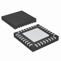
MAX1904ETJ+ Maxim Integrated Products, MAX1904ETJ+ Datasheet - Page 25

MAX1904ETJ+
Manufacturer Part Number
MAX1904ETJ+
Description
IC CNTRLR PWR SPLY LN 32-TQFN
Manufacturer
Maxim Integrated Products
Datasheet
1.MAX1904ETJ.pdf
(33 pages)
Specifications of MAX1904ETJ+
Applications
Controller, Notebook Computers
Voltage - Input
4.2 ~ 30 V
Number Of Outputs
4
Voltage - Output
2.5 ~ 5 V
Operating Temperature
0°C ~ 85°C
Mounting Type
Surface Mount
Package / Case
32-TQFN Exposed Pad
Output Voltage
3.3 V, 5 V, 2.5 V to 5.5 V
Output Current
5 A
Input Voltage
4.2 V to 30 V
Mounting Style
SMD/SMT
Maximum Operating Temperature
+ 85 C
Minimum Operating Temperature
- 40 C
Lead Free Status / RoHS Status
Lead free / RoHS Compliant
Table 5. Low-Voltage Troubleshooting Chart
where C
high-side MOSFET (a data sheet parameter), I
the DH gate-driver peak output current (1.5A typical),
and 20ns is the rise/fall time of the DH driver (20ns typ).
where V
Q
and high-side switches. For matched MOSFETs, Q
twice the data sheet value of an individual MOSFET. If
V
tion with V
improved by connecting V
such as the system 5V supply:
Sag or droop in V
under step-load change
Dropout voltage is too
high (V
V
Unstable—jitters between
different duty factors and
frequencies
Secondary output won’t
support a load
Poor efficiency
Won’t start under load or
quits before battery is
completely dead
OUT
G
IN
500kHz Multi-Output, Low-Noise Power-Supply
is the sum of the gate-charge values for low-side
decreases)
is set to less than 4.5V, replace V
OUT
SYMPTOM
L
RSS
is the internal-logic-supply voltage (5V), and
P tran
P(diode) = I
follows V
f
(
BATT
×
is the reverse transfer capacitance of the
3
2
OUT
)
×
P(gate) = Q
=
. In this case, efficiency can be
______________________________________________________________________________________
[
IN
V
(
V
IN
as
IN
×
LOAD
×
I
LOAD
C
Low V
differential, <1.5V
Low V
differential, <1V
Low V
differential, <0.5V
Low V
differential,
V
V
Low input voltage,
<5V
Low input voltage,
<4.5V
RSS GATE
L
IN
OUT(MAIN)
Controllers for Notebook Computers
G
✕
to an efficient 5V source,
< 1.3
×
/
CONDITION
✕
V
I
IN
IN
IN
IN
FWD
f
- V
✕
- V
- V
- V
✕
V
)
OUT
OUT
OUT
OUT
-
✕
L
20
t
D
ns
L
✕
]
in this equa-
f
GATE
Limited inductor-current slew rate
per cycle.
Maximum duty-cycle limits
exceeded.
Normal function of internal low-
dropout circuitry.
Not enough duty cycle left to
initiate forward-mode operation.
Small AC current in primary can’t
store energy for flyback
operation.
V
dropout and isn’t providing good
gate-drive levels.
V
V
L
L
L
linear regulator is going into
output is so low that it hits the
UVLO threshold.
G
is
is
ROOT CAUSE
where t
V
This power is dissipated in the MOSFET body diode if
no external Schottky diode is used:
where I
Design Procedure and Input-Capacitor Value sections.
Under light loads, the PWM operates in discontinuous
mode, where the inductor current discharges to zero at
some point during the switching cycle. This makes the
inductor current’s AC component high compared to the
load current, which increases core losses and I
es in the output filter capacitors. For best light-load effi-
ciency, use MOSFETs with moderate gate-charge
levels, and use ferrite, MPP, or other low-loss core
material.
FWD
is the forward voltage of the diode.
RMS
D
Light-Load Efficiency Considerations
is the diode-conduction time (120ns typ) and
is the input ripple current as calculated in the
P(cap) = (I
Increase bulk output capacitance per
formula (see the Low-Voltage Operation
section). Reduce inductor value.
Reduce operation to 333kHz. Reduce
MOSFET on-resistance and coil DCR.
Increase the minimum input voltage or
ignore.
Reduce operation to 333kHz. Reduce
secondary impedances; use a Schottky
diode, if possible. Stack secondary
winding on the main output.
Use a small 20mA Schottky diode for
boost diode. Supply V
source.
Supply V
than V
IN
RMS
, such as the system 5V supply.
L
from an external source other
)
2
SOLUTION
x R
ESR
L
from an external
2
R loss-
25


