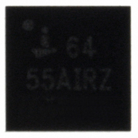
ISL6455AIRZ-TK Intersil, ISL6455AIRZ-TK Datasheet - Page 9

ISL6455AIRZ-TK
Manufacturer Part Number
ISL6455AIRZ-TK
Description
IC REG TRPL SYNCH DUAL LDO 24QFN
Manufacturer
Intersil
Datasheet
1.ISL6455IRZ-TK.pdf
(12 pages)
Specifications of ISL6455AIRZ-TK
Applications
Converter, FPGAs
Voltage - Input
4.2 ~ 5.5 V
Number Of Outputs
3
Voltage - Output
0.8 ~ 3.3 V
Operating Temperature
-40°C ~ 85°C
Mounting Type
Surface Mount
Package / Case
24-VQFN Exposed Pad, 24-HVQFN, 24-SQFN, 24-DHVQFN
Lead Free Status / RoHS Status
Lead free / RoHS Compliant
Other names
ISL6455AIRZ-TKTR
Available stocks
Company
Part Number
Manufacturer
Quantity
Price
Company:
Part Number:
ISL6455AIRZ-TK
Manufacturer:
Intersil
Quantity:
2 100
sensed via an internal circuit. The error amplifier sets the
threshold for the PWM comparator. The high side switch is
turned off when the sensed inductor current reaches this
threshold. After a minimum dead time preventing shoot
through current, the low side N-channel MOSFET will be
turned on and the current ramps down again. As the clock
cycle is completed, the low side switch will be turned off and
the next clock cycle starts.
The control loop is internally compensated reducing the
amount of external components.
The switch current is internally sensed and the maximum
peak current limit is 1300mA.
Synchronization
The typical operating frequency for the converter is 750kHz
if no clock signal is applied to SYNC pin. It is possible to
synchronize the converter to an external clock within a
frequency range from 500kHz to 1MHz. The device
automatically detects the rising edge of the first clock and
will synchronize immediately to the external clock. If the
clock signal is stopped, the converter automatically switches
back to the internal clock and continues operation without
interruption. The switch over will be initiated if no rising edge
on the SYNC pin is detected for a duration of two internal
1.3µs clock cycles.
Soft-Start
As the EN (Enable) pin goes high, the soft-start function will
generate an internal voltage ramp. This causes the start-up
current to slowly rise preventing output voltage overshoot
and high inrush currents. The soft-start duration is typically
5.5ms with 750kHz switching frequency. When the soft-start
is completed, the error amplifier will be connected directly to
the internal voltage reference. The SYNC input is ignored
during soft-start.
Enable PWM
Logic low on EN pin forces the PWM section into shutdown.
In shutdown all the major blocks of the PWM including power
switches, drivers, voltage reference, and oscillator are
turned off.
Power Good (PG_PWM)
When chip is enabled, this output is asserted HIGH, when
V
this range. When the PWM is disabled, the output is active
low.
Leave the PG_PWM pin unconnected when not used.
PWM Overvoltage and Overcurrent Protection
The PWM output current is sampled at the end of each PWM
cycle. Should it exceed the overcurrent limit, a 4 bit up/down
counter counts up two LSB. Should it not be in overcurrent
the counter counts down one LSB (but the counter will not
"rollover" or count below 0000). If >33% of the PWM cycles
go into overcurrent, the counter rapidly reaches count 1111
OUT
is within 8% of Vopwm value and active low outside
9
ISL6455, ISL6455A
and the PWM output is shut down and the soft-start counter
is reset. After 16 clocks the PWM output is enabled and the
SS cycle is started.
If V
clock cycles, the PWM output is shut off and the SS counters
reset. The chip waits for the output voltage to go below
undervoltage (8% below nominal) the goes through two
dummy soft-start cycles (PWM disabled for 2 SS cycles =
11ms) and then starts a normal soft-start cycle.
PG_LDO
PG_LDO is an open drain pulldown NMOS output that will
sink 1mA at 0.4V maximum. It goes to the active low state if
either LDO output is out of regulation by a value greater than
15%. When the LDO is disabled, the output is active low.
LDO Regulators
Each LDO consists of a 1.184V reference, error amplifier,
MOSFET driver, P-Channel pass transistor, dual-mode
comparator. The voltage is set by means of two resistors the
Ra and Rb for LDO2 and Rc and Rd for LDO1. The 1.184V
band gap reference is connected to the error amplifier’s
inverting input. The error amplifier compares this reference
to the selected feedback voltage and amplifies the
difference. The MOSFET driver reads the error signal and
applies the appropriate drive to the P-Channel pass
transistor. If the feedback voltage is lower than the reference
voltage, the pass transistor gate is pulled lower, allowing
more current to pass and increasing the output voltage. If the
feedback voltage is higher then the reference voltage, the
pass transistor gate is driven higher, allowing less current to
pass to the output.
Internal P-Channel Pass Transistors
Both the LDO Regulators in ISL6455 feature a typical 0.5Ω
r
several advantages over similar designs using PNP bipolar
pass transistors. The P-Channel MOSFET requires no base
drive, which reduces quiescent current considerably. PNP
based regulators waste considerable current in dropout
when the pass transistor saturates. They also use high base
drive currents under large loads. The ISL6455 does not have
these drawbacks.
Integrated RESET for MAC/Baseband Processors
The ISL6455 includes a microprocessor supervisory block.
This block eliminates an extra RESET IC and external
components needed in wireless chipset applications. This
block performs a single function; it asserts a RESET signal
whenever the VIN_PWM supply voltage decreases below a
preset threshold, and keeps it asserted for a programmable
time period set by the external capacitor CT.
UVLO Reset threshold is always lower than the RESET
threshold. This insures that as V
before the LDOs and PWM are shut off.
DS(on)
OUT
P-channel MOSFET pass transistor. This provides
exceeds the overvoltage limit for 32 consecutive
IN
falls, the reset goes low
December 21, 2005
FN9196.0


